POWER7
Topic: Engineering
 From HandWiki - Reading time: 8 min
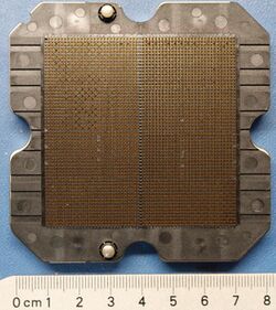
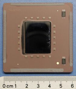 IBM Power7 4 GHz 8-way CPU (de-lidded) from an IBM 9119 | |
| General Info | |
|---|---|
| Launched | 2010 |
| Designed by | IBM |
| Performance | |
| Max. CPU clock rate | 2.4 GHz to 4.25 GHz |
| Cache | |
| L1 cache | 32+32 KB/core |
| L2 cache | 256 KB/core |
| L3 cache | 4 MB/core |
| Architecture and classification | |
| Min. feature size | 45 nm |
| Instruction set | Power ISA (Power ISA v.2.06) |
| Physical specifications | |
| Cores |
|
| History | |
| Predecessor | POWER6 |
| Successor | POWER8 |
| POWER, PowerPC, and Power ISA architectures |
|---|
| NXP (formerly Freescale and Motorola) |
| IBM |
|
| IBM/Nintendo |
| Other |
| Related links |
| Cancelled in gray, historic in italic |
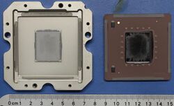
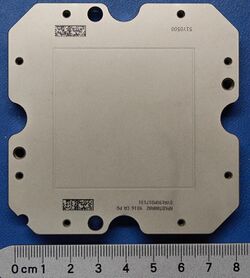
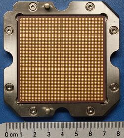
POWER7 is a family of superscalar multi-core microprocessors based on the Power ISA 2.06 instruction set architecture released in 2010 that succeeded the POWER6 and POWER6+. POWER7 was developed by IBM at several sites including IBM's Rochester, MN; Austin, TX; Essex Junction, VT; T. J. Watson Research Center, NY; Bromont, QC[1] and IBM Deutschland Research & Development GmbH, Böblingen, Germany laboratories. IBM announced servers based on POWER7 on 8 February 2010.[2][3]
History
IBM won a $244 million DARPA contract in November 2006 to develop a petascale supercomputer architecture before the end of 2010 in the HPCS project. The contract also states that the architecture shall be available commercially. IBM's proposal, PERCS (Productive, Easy-to-use, Reliable Computer System), which won them the contract, is based on the POWER7 processor, AIX operating system and General Parallel File System.[4]
One feature that IBM and DARPA collaborated on is modifying the addressing and page table hardware to support global shared memory space for POWER7 clusters. This enables research scientists to program a cluster as if it were a single system, without using message passing. From a productivity standpoint, this is essential since some scientists are not conversant with MPI or other parallel programming techniques used in clusters.[5]
Design
The POWER7 superscalar multi-core architecture was a substantial evolution from the POWER6 design, focusing more on power efficiency through multiple cores and simultaneous multithreading (SMT).[6] The POWER6 architecture was built from the ground up to maximize processor frequency at the cost of power efficiency. It achieved a remarkable 5 GHz. While the POWER6 features a dual-core processor, each capable of two-way simultaneous multithreading (SMT), the IBM POWER 7 processor has up to eight cores, and four threads per core, for a total capacity of 32 simultaneous threads.[7]
IBM stated at ISCA 29[8] that peak performance was achieved by high frequency designs with 10–20 FO4 delays per pipeline stage at the cost of power efficiency. However, the POWER6 binary floating-point unit achieves a "6-cycle, 13-FO4 pipeline".Cite error: Closing </ref> missing for <ref> tag There is also a special TurboCore mode that can turn off half of the cores from an eight-core processor, but those 4 cores have access to all the memory controllers and L3 cache at increased clock speeds. This makes each core's performance higher which is important for workloads which require the fastest sequential performance at the cost of reduced parallel performance. TurboCore mode can reduce "software costs in half for those applications that are licensed per core, while increasing per core performance from that software."[9] The new IBM Power 780 scalable, high-end servers featuring the new TurboCore workload optimizing mode and delivering up to double performance per core of POWER6 based systems.[9]
Each core is capable of four-way simultaneous multithreading (SMT). The POWER7 has approximately 1.2 billion transistors and is 567 mm2 large fabricated on a 45 nm process. A notable difference from POWER6 is that the POWER7 executes instructions out-of-order instead of in-order. Despite the decrease in maximum frequency compared to POWER6 (4.25 GHz vs 5.0 GHz), each core has higher performance than the POWER6, while each processor has up to 4 times the number of cores.
POWER7 has these specifications:[10][11]
- 45 nm SOI process, 567 mm2
- 1.2 billion transistors
- 3.0–4.25 GHz clock speed
- max 4 chips per quad-chip module
- 4, 6 or 8 C1 cores per chip
- 4 SMT threads per C1 core (available in AIX 6.1 TL05 (releases in April 2010) and above)
- 12 execution units per C1 core:
- 2 fixed-point units
- 2 load/store units
- 4 double-precision floating-point units
- 1 vector unit supporting VSX
- 1 decimal floating-point unit
- 1 branch unit
- 1 condition register unit
- 32+32 KB L1 instruction and data cache (per core)[12]
- 256 KB L2 Cache (per C1 core)
- 4 MB L3 cache per C1 core with maximum up to 32 MB supported. The cache is implemented in eDRAM, which does not require as many transistors per cell as a standard SRAM[5] so it allows for a larger cache while using the same area as SRAM.
- 4, 6 or 8 C1 cores per chip
The technical specification further specifies:[13]
Each POWER7 processor core implements aggressive out-of-order (OoO) instruction execution to drive high efficiency in the use of available execution paths. The POWER7 processor has an Instruction Sequence Unit that is capable of dispatching up to six instructions per cycle to a set of queues. Up to eight instructions per cycle can be issued to the Instruction Execution units.
This gives the following theoretical single precision (SP) performance figures (based on a 4.14 GHz 8 core implementation):
- max 99.36 GFLOPS per core
- max 794.88 GFLOPS per chip
4 64-bit SIMD units per core, and a 128-bit SIMD VMX unit per core, can do 12 Multiply-Adds per cycle, giving 24 SP FP ops per cycle. At 4.14 GHz, that gives 4.14 billion * 24 = 99.36 SP GFLOPS, and at 8 cores, 794.88 SP GFLOPS.
Peak double precision (DP) performance is roughly half of peak SP performance.
For comparison, Intel's 2013 Haswell architecture CPUs can do 16 DP FLOPs or 32 SP FLOPs per cycle (8/16 DP/SP fused multiply-add spread across 2× 256-bit AVX2 FP vector units).[14] At 3.4 GHz (i7-4770) this translates into 108.8 SP GFLOPS per core and 435.2 SP GFLOPS peak performance across the 4-core chip, giving roughly similar levels of performance per core, without taking into account the effects or benefits of Intel's Turbo Boost technology.
This theoretical peak performance comparison holds in practice too, with the POWER7 and the i7-4770 obtaining similar scores in the SPEC CPU2006 floating point benchmarks (single-threaded): 71.5[15] for POWER7 versus 74.0[16] for i7-4770.
Notice that the POWER7 chip significantly outperformed (2×–5×) the i7 in some benchmarks (bwaves, cactusADM, lbm) while also being significantly slower (2x-3x) in most others. This is indicative of major architectural differences between the two chips / mainboards / memory systems etc.: they were designed with different workloads in mind.
However, overall, in a very broad sense, one can say that the floating-point performance of the POWER7 is similar to that of the Haswell i7.
POWER7+
IBM introduced the POWER7+ processor at the Hot Chips 24 conference in August 2012. It is an updated version with higher speeds, more cache and integrated accelerators. It is manufactured on a 32 nm fabrication process.[17]
The first boxes to ship with the POWER7+ processors were IBM Power 770 and 780 servers. The chips have up to 80 MB of L3 cache (10 MB/core), improved clock speeds (up to 4.4 GHz) and 20 LPARs per core.[18]
Products
As of October 2011[update], the range of POWER7-based systems including IBM Power Systems "Express" models (710, 720, 730, 740 and 750), Enterprise models (770, 780 and 795) and High Performance computing models (755 and 775). Enterprise models differ in having Capacity on Demand capabilities. Maximum specifications are shown in the table below.
| Name | Number of sockets | Number of cores | CPU clock frequency |
|---|---|---|---|
| 710 Express | 1 | 6 | 4.2 GHz |
| 710 Express | 1 | 8 | 4.2 GHz |
| 720 Express (8202-E4B, POWER7)[19] | 1 | 8 | 3.0 GHz |
| 720 Express (8202-E4D, POWER7+)[20] | 1 | 8 | 3.6 GHz |
| 730 Express | 2 | 12 | 4.2 GHz |
| 730 Express | 2 | 16 | 3.6 GHz or 4.2 GHz |
| 740 Express | 2 | 12 | 4.2 GHz |
| 740 Express | 2 | 16 | 3.6 GHz or 4.2 GHz |
| 750 Express | 4 | 24 | 3.72 GHz |
| 750 Express | 4 | 32 | 3.22 GHz or 3.61 GHz |
| 755 | 4 | 32 | 3.61 GHz |
| 770 | 8 | 48 | 3.7 GHz |
| 770 | 8 | 64 | 3.3 GHz |
| 775 (Per Node) | 32 | 256 | 3.83 GHz |
| 780 (MaxCore mode) | 8 | 64 | 3.92 GHz |
| 780 (TurboCore mode) | 8 | 32 | 4.14 GHz |
| 780 (4 Socket Node) | 16 | 96 | 3.44 GHz |
| 795 | 32 | 192 | 3.72 GHz |
| 795 (MaxCore mode) | 32 | 256 | 4.0 GHz |
| 795 (TurboCore mode) | 32 | 128 | 4.25 GHz |
IBM also offers 5 POWER7 based BladeCenters.[21] Specifications are shown in the table below.
| Name | Number of cores | CPU clock frequency | Blade slots required |
|---|---|---|---|
| BladeCenter PS700 | 4 | 3.0 GHz | 1 |
| BladeCenter PS701 | 8 | 3.0 GHz | 1 |
| BladeCenter PS702 | 16 | 3.0 GHz | 2 |
| BladeCenter PS703 | 16 | 2.4 GHz | 1 |
| BladeCenter PS704 | 32 | 2.4 GHz | 2 |
The following are supercomputer projects that use the POWER7 processor:
See also
References
- ↑ Authier, Isabelle (2011-02-17). "IBM Bromont au coeur de Watson" (in French). Cyberpresse. Cyberpresse. http://www.cyberpresse.ca/la-voix-de-lest/actualites/201102/16/01-4370783-ibm-bromont-au-coeur-de-watson.php.
- ↑ "IBM Unveils New POWER7 Systems To Manage Increasingly Data-Intensive Services". IBM. 2010-02-08. http://www-03.ibm.com/press/us/en/pressrelease/29315.wss.
- ↑ "New POWER7 workload optimizing systems". YouTube. IBM. 2010-02-05. https://www.youtube.com/watch?v=CmXfZmplxUA.
- ↑ "Cray, IBM picked for U.S. petaflop computer effort". EE Times. https://www.eetimes.com/cray-ibm-picked-for-u-s-petaflop-computer-effort/.
- ↑ 5.0 5.1 "Hot Chips XXI Preview". Real World Technologies. http://realworldtech.com/page.cfm?ArticleID=RWT081209143650&p=2.
- ↑ Kanter, David. "New Information on POWER7". http://realworldtech.com/page.cfm?ArticleID=RWT081209143650&p=2.
- ↑ Varhol, Peter (9 February 2010). "IBM Launches POWER 7 Processor February 9, 2010". http://pvarhol.wordpress.com/2010/02/09/ibm-launches-power-7-processor/.
- ↑ "ISCA 29 Conference Notes". http://www.realworldtech.com/page.cfm?ArticleID=RWT053002100716.
- ↑ 9.0 9.1 "IBM Unveils New POWER7 Systems To Manage Increasingly Data-Intensive Services". IBM.com. http://www-03.ibm.com/press/us/en/pressrelease/29315.wss.
- ↑ "IBM in Education – Business & Technology Solutions". IBM. http://www.it.utah.edu/leadership/committees/IT_Managers/papers/IBMinEducation.ppt.
- ↑ "IBM's 8-core POWER7: twice the muscle, half the transistors". Ars Technica. September 2009. https://arstechnica.com/hardware/news/2009/09/ibms-8-core-power7-twice-the-muscle-half-the-transistors.ars.
- ↑ "Bluewater HW specifications". National Center for Supercomputing Applications. http://www.ncsa.illinois.edu/BlueWaters/hardware.html.
- ↑ "IBM Power 770 and 780 Technical Overview and Introduction". IBM. http://www.redbooks.ibm.com/redpapers/pdfs/redp4639.pdf.
- ↑ Anand Lal Shimpi (5 October 2012). "Intel's Haswell Architecture Analyzed: Building a New PC and a New Intel". http://www.anandtech.com/show/6355/intels-haswell-architecture.
- ↑ "SPEC CFP2006 Result, IBM Power 780 Server (3.86 GHz, 16 core)". https://www.spec.org/cpu2006/results/res2010q2/cpu2006-20100426-10752.html.
- ↑ "SPEC CFP2006 Result, Intel DH87MC Motherboard (Intel Core i7-4770)". https://www.spec.org/cpu2006/results/res2014q3/cpu2006-20140728-30673.html.
- ↑ "Hot Chips: Update für IBMs Power7". http://www.heise.de/ct/meldung/Hot-Chips-Update-fuer-IBMs-Power7-1679075.html.
- ↑ Morgan, Timothy Prickett (3 October 2012). "Power7+ chips debut in fat IBM midrange systems". https://www.theregister.com/2012/10/03/ibm_power7_plus_server_launch/.
- ↑ "IBM Power 720 and 740 Technical Overview and Introduction". IBM. 2012-12-03. p. 9. http://redbooks.ibm.com/redpapers/pdfs/redp4637.pdf.
- ↑ "IBM Power 720 and 740 Technical Overview and Introduction". IBM. 2013-05-16. p. 9. http://redbooks.ibm.com/redpapers/pdfs/redp4984.pdf.
- ↑ "IBM Power Systems hardware - Blade servers". IBM. http://www-03.ibm.com/systems/power/hardware/blades/index.html.
External links
- IBM POWER7 Systems - IBM POWER7 product page
- IBM POWER7 Technology and Systems - IBM Journal of Research and Development (published by IEEE Xplore)
- IBM Won DARPA HPCS Phase-III
- IBM Won DARPA HPCS Phase-II
- IBM Has Its PERCS
- POWER 780 SPECint_rate_base2006 result
- IBM BladeCenter PS703 and PS704 Technical Overview and Introduction
 |
 KSF
KSF