Switching control techniques
Topic: Engineering
 From HandWiki - Reading time: 7 min
Switching Control Techniques address electromagnetic interference (EMI) mitigation on power electronics (PE). The design of power electronics involves overcoming three key challenges:[1]
- power losses
- EMI
- harmonics
Also, the use of PE introduces crucial drawbacks into the electrical grid regarding the EMI, that must be considered during its design and operation, especially when is desirable to meet the EMC constraints (e.g., CISPR 22). Dealing with static converters designed with PE, for example, can causes signal disturbances in the electromagnetic environment (near or far fields), e.g. with respect to radio receivers, vehicle navigation systems, avionics, etc.[2]
Those disturbances are caused mainly by the high frequency interference from the semiconductor switching components inside PE. It is challenging to handle this aspect with filtering and shielding techniques as the demands for cost and size for its implementation increase, along with greater efficiency. Therefore, switching mode power supplies are used instead in order to obtain a higher efficiency.[3]
Mitigation of electromagnetic interference
The breakthrough of semiconductor technologies[4] and their adoption in power electronics devices [5] provides fast power switching devices off the shelf with progressively increasing efficiency and high-density power technology in electronics systems. In order to reach the EMC requirements, it is important to better understand the dynamics behavior of the switching devices in PE and the factors which causes modifications on output waveform shaping and rate.[6] Therefore, it is possible to distinguish two techniques of EMI suppression regarding the PEI (Power Electronics Interface) (Fig. 1): reduce the emissions at the source or make the propagation path less effective. On one hand, intervening on the source is possible by using switching control techniques (increasing the efficiency), redesigning the circuit (costly and time demanding) and using soft switching transition. On the other hand, by adding external or internal filters (also costly) it is possible to address the propagation path.

Considering that handling the electric supply is not necessary in order to modify the internal circuitry of the electronic device, e.g. inverter, converter, rectifier, so on (then cutting off costs), by using switching control techniques it is possible to increase the efficiency of the PE. Although the use of switching transistors can increase of conducted emissions generated by the power supply, it can enhance the efficiency of the controllers (e.g. as used by high-efficiency controllers). Once the fundamental component of the waveform is associated to conversion of energy (either DC or AC) and the switching frequency (even dozens of kiloHertz or above), the choice of convenient waveform profile is made regarding to the target and the PE converter constraints.[7][8]
Thus, the high efficiency reached by the switching power converters is related to the use of switching devices, energy storage elements and transformers, through proper modulation activity of the switches to convert the available DC or AC and voltage or current signal waveforms of the power source into the AC or DC waveforms needed by the load. Those switching devices are mostly semiconductors such as: transistors, diodes, thyristors, Field-effect transistor etc.[8] The high performance of switching devices is the main reason for searching an appropriate switching control technique. The two most popular methods are:[9][10]
- Deterministic, in which pulse-width modulation (PWM) is applicable as programmed switching method and;
- Non-deterministic (or random modulation), characterized by the random PWM (RPWM) method.
The key distinction between these techniques is attributed to the fact that randomness introduces EMI noise with a spectrum continuously distributed over frequency, i.e. a uniform power across the frequency band.
Deterministic modulation

PWM is considered the most common deterministic technique. Considering the example of a DC-DC converter, a controlled switch is designed to “cut-off” the DC waveform into a pulse-shaped waveform. Therefore, the voltage of this signal alternates at the switching frequency between a maximum value and zero. The converter also controls the duty cycle (𝐷), that is, the time frame in which the switch device is turned off in each cycle.[7][8][11] Generally, the waveform of the power electronics interface (PEI) is a steady-state periodic time function.
By the middle of 1990s, some researchers started to evaluate which frequency modulation techniques to apply to reduce EMI emissions, focusing on communications and microprocessor systems.[8][11] The main concern with these latter approaches is that EMI is equally spread along the whole frequency spectrum, and these approaches do not provide any control over the bands where EMI energy is spread. This feature is crucial for telecommunications, telematics, and automation systems applications, where EMI at specific selective frequencies must be avoided. Investigations of such techniques applied to EMI reduction of digital systems is a subject of significant concern, included the introduction of a new area of research with modulation techniques to power electronics converters with randomized modulation.
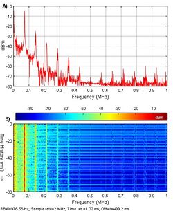
As an exemplification, Fig. 2.A at shows the spectrum and Fig. 2.B shows the spectrogram of EMI shaped-noise voltage output for a programmable PWM with switching frequency in a buck converter with 𝐷 = 0.50, in accordance with CISPR A standard. According to Fig. 2.A, the programmable switching frequency creates a significant impact by the EMI noise shape as well as the high sideband. Fig. 2.B shows the high peaks amplitude of EMI noise, at the switching frequency and their multiple harmonics.
Non-deterministic modulation

The randomness process can be performed by spreading the harmonics power existing at well-defined frequencies (i.e. discrete harmonics) through a wide range of frequencies in order to remove harmonic components of significant magnitude. With that, discrete harmonics are substantially decreased, and the harmonic power is extended across the whole spectrum as noise.[12][13][14]
The procedure behind of most randomized modulation is related to the schemes of successive randomization of the switching pulse train (or its segments), which are independent statistically and ruled by probabilistic rules. So, the randomized modulation procedure must enable accurate control of the time-domain performance of randomized switching, in addition to spectral shaping in the frequency domain. The elementary analysis problem in randomized modulation regards the spectral characteristics of the signal (and associated waveforms) in a converter to the probabilistic structure that governs the dithering of an underlying deterministic nominal switching pattern.
In this case, the suitable approach is to analyse the randomized switching setup in the power spectrum, computed from the fourier transform (FT) of the original signal auto correlation. Note that the FT of a random signal is itself a random function, i.e., it is a random variable at each frequency. The power spectrum, on the other hand, owns convergence properties and can be estimated reliably from the available signal.[8][15]
Therefore, it is possible to categorize the randomized modulation strategies as stationary.
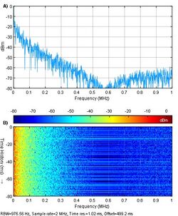
The Fig. 3.A shows the spectrum of EMI noise shape of voltage output for RPWM with the switching frequency implemented in one Buck-Converter, and in accordance with CISPR A standard. It shows the spectrogram of EMI noise shape of voltage output for an RPWM, where it is possible to note (also in Fig. 3. A) that aleatory process inserts the continuous EMI noise shape, in low-frequencies, the EMI noise shape follows oscillatory mode with their noise value decreasing across the spectrum. Fig. 3.B, shows the spectrogram of EMI noise shape of voltage output for an RPWM, where it is possible to note (also in Fig. 3.A) that randomization process introduces the continuous EMI noise shape, and in low-frequencies, the EMI noise shape follows oscillatory mode with their noise value decreasing across the spectrum.
See also
- Power Electronics
- Electromagnetic Interference
- Electromagnetic Compatibility
- Random modulation
- List of common EMC test standards
References
- ↑ Kroposki, Benjamin; Pink, Christopher; DeBlasio, Richard; Thomas, Holly; Simões, Marcelo; Sen, Pankaj K. (September 2010). "Benefits of Power Electronic Interfaces for Distributed Energy Systems". IEEE Transactions on Energy Conversion 25 (3): 901–908. doi:10.1109/TEC.2010.2053975. Bibcode: 2010ITEnC..25..901K.
- ↑ Costa, Francois (2014). Electromagnetic compatibility in power electronics. ISTE. ISBN 978-1-84821-504-7.
- ↑ Niu, Junying (2016). "Suppressing Electromagnetic Interference in Switching-Mode Power Supplies by Chaotic Carrier Frequency Modulation" (in de). https://ub-deposit.fernuni-hagen.de/receive/mir_mods_00000799. Retrieved 25 June 2020.
- ↑ Zare, Firuz (14 October 2008). "EMC and modern power electronic systems Section 5: Multilevel converters". 2008 IEEE International Symposium on Electromagnetic Compatibility. pp. 1–8. doi:10.1109/ISEMC.2008.4652183. ISBN 978-1-4244-1699-8.
- ↑ Chakraborty, Sudipta; Kramer, Bill; Kroposki, Benjamin (December 2009). "A review of power electronics interfaces for distributed energy systems towards achieving low-cost modular design". Renewable and Sustainable Energy Reviews 13 (9): 2323–2335. doi:10.1016/j.rser.2009.05.005. Bibcode: 2009RSERv..13.2323C.
- ↑ Koyama, Yoshitsugu; Tanaka, Mitsuhiro; Akagi, Hirofumi (2010). "Modeling and analysis for simulation of common-mode noises produced by an inverter-driven air conditioner". The 2010 International Power Electronics Conference - ECCE ASIA -. pp. 2877–2883. doi:10.1109/IPEC.2010.5544592. ISBN 978-1-4244-5394-8.
- ↑ 7.0 7.1 Balcells, J.; Santolaria, A.; Orlandi, A.; Gonzalez, D.; Gago, J. (August 2005). "EMI Reduction in Switched Power Converters Using Frequency Modulation Techniques". IEEE Transactions on Electromagnetic Compatibility 47 (3): 569–576. doi:10.1109/TEMC.2005.851733. Bibcode: 2005ITElC..47..569B.
- ↑ 8.0 8.1 8.2 8.3 8.4 Stankovic, A.A.; Lev-Ari, H. (May 2002). "Randomized modulation in power electronic converters". Proceedings of the IEEE 90 (5): 782–799. doi:10.1109/JPROC.2002.1015007. Bibcode: 2002IEEEP..90..782S.
- ↑ Trzynadlowski, A.M.; Wang, Zhiqiang; Nagashima, J.; Stancu, C. (10 December 2002). "Comparative investigation of PWM techniques for general motors' new drive for electric vehicles". Conference Record of the 2002 IEEE Industry Applications Conference. 37th IAS Annual Meeting (Cat. No.02CH37344). 3. pp. 2010–2015. doi:10.1109/IAS.2002.1043808. ISBN 0-7803-7420-7.
- ↑ Kazmierkowski, Marian P.; Krishnan, Ramu; Blaabjerg, Frede (2002). Control in power electronics : selected problems. Academic Press. ISBN 9780080490786.
- ↑ 11.0 11.1 Hardin, K.B.; Fessler, J.T.; Bush, D.R. (1994). "Spread spectrum clock generation for the reduction of radiated emissions". Proceedings of IEEE Symposium on Electromagnetic Compatibility. pp. 227–231. doi:10.1109/ISEMC.1994.385656. ISBN 0-7803-1398-4. https://ieeexplore.ieee.org/document/385656/authors#authors.
- ↑ Hui, S.Y.; Shrivastava, Y.; Sathiakumar, S.; Tse, K.K.; Henry Shu-Hung Chun (November 1998). "A comparison of nondeterministic and deterministic switching methods for DC-DC power converters". IEEE Transactions on Power Electronics 13 (6): 1046–1055. doi:10.1109/63.728332. Bibcode: 1998ITPE...13.1046H.
- ↑ Lezynski, Piotr; Smolenski, Robert; Loschi, Hermes; Thomas, Dave; Moonen, Niek (February 2020). "A novel method for EMI evaluation in random modulated power electronic converters". Measurement 151. doi:10.1016/j.measurement.2019.107098. Bibcode: 2020Meas..15107098L.
- ↑ Loschi, Hermes; Lezynski, Piotr; Smolenski, Robert; Nascimento, Douglas; Sleszynski, Wojciech (11 May 2020). "FPGA-Based System for Electromagnetic Interference Evaluation in Random Modulated DC/DC Converters". Energies 13 (9): 2389. doi:10.3390/en13092389.
- ↑ Proakis, J. G.; Manolakis, D. G. (1992). Digital signal processing : principles, algorithms, and applications (3rd ed.). Prentice Hall. ISBN 978-0133737622.
 |
 KSF
KSF