Nano and Micro Devices Center
Topic: Organization
 From HandWiki - Reading time: 2 min
 | |
| Type | Research Center |
|---|---|
| Established | 2008 |
| Chairman | Robert Lindquist |
| Director | John D. Williams |
Academic staff | 10 |
Administrative staff | 6 |
| Postgraduates | 16 |
| Location | Huntsville, Alabama , [ ⚑ ] : 34°43′22″N 86°38′19″W / 34.72278°N 86.63861°W |
| Campus | University of Alabama in Huntsville main campus |
| Website | http://nmdc.uah.edu |
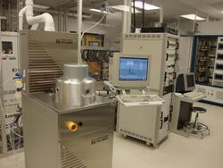
The Nano and Micro Devices Center (NMDC) is a research center located at the University of Alabama in Huntsville. The center forms the backbone of nanotechnology research in the university. It operates a level 4 clean room as well as several other lab facilities.
Objectives
The objective of the center is to effectively integrate the expertise in electrical, chemical, and materials engineering, biology, chemistry and physics towards the development and research in the fields of micro electro-mechanical systems (MEMS) and nanotechnology.[1][2]
Facilities

The center operates a clean room that is equipped with microfabrication machines that perform thin film deposition, photolithography, dry and wet etching, and metrology measurements. It also operates a dark room for wet etching, electroplating and porous silicon fabrication. The facilities are utilized by organizations based in north Alabama. The processes performed in such a clean room level may be classified into:[3]
- Lithography: the processes under this category include the conventional UV-lithographic techniques, Electron Beam lithography, and Projection lithography.
- Material Deposition processes: under this category fall the processes of Sputtering, thermal vapor deposition, and electroplating, other techniques to deposit biological molecules and bilayer membranes include the Langmuir- Blodgett technique.
- Material Removal Processes: these include dry etching such as reactive ion etching, or wet etching such as anisotropic etching of silicon in a KOH bath.
- Surface Analysis and Characterization: such as Atomic Force Microscopy, Scanning Electron Microscopy, Confocal Microsocopy, Ellipsometry, UV, IR, and Raman Spectroscopy, X-ray Spectroscopy, and other techniques.
- Computing
References
Template:University of Alabama in Huntsville
 |
 KSF
KSF