Work function
Topic: Physics
 From HandWiki - Reading time: 15 min
In solid-state physics, the work function (sometimes spelled workfunction) is the minimum thermodynamic work (i.e., energy) needed to remove an electron from a solid to a point in the vacuum immediately outside the solid surface. Here "immediately" means that the final electron position is far from the surface on the atomic scale, but still too close to the solid to be influenced by ambient electric fields in the vacuum. The work function is not a characteristic of a bulk material, but rather a property of the surface of the material (depending on crystal face and contamination).
Definition
The work function W for a given surface is defined by the difference[1]
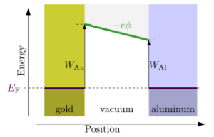
where −e is the charge of an electron, ϕ is the electrostatic potential in the vacuum nearby the surface, and EF is the Fermi level (electrochemical potential of electrons) inside the material. The term −eϕ is the energy of an electron at rest in the vacuum nearby the surface.

In practice, one directly controls EF by the voltage applied to the material through electrodes, and the work function is generally a fixed characteristic of the surface material. Consequently, this means that when a voltage is applied to a material, the electrostatic potential ϕ produced in the vacuum will be somewhat lower than the applied voltage, the difference depending on the work function of the material surface. Rearranging the above equation, one has
where V = −EF / e is the voltage of the material (as measured by a voltmeter, through an attached electrode), relative to an electrical ground that is defined as having zero Fermi level. The fact that ϕ depends on the material surface means that the space between two dissimilar conductors will have a built-in electric field, when those conductors are in total equilibrium with each other (electrically shorted to each other, and with equal temperatures).
The work function refers to removal of an electron to a position that is far enough from the surface (many nm) that the force between the electron and its image charge in the surface can be neglected.[1] The electron must also be close to the surface compared to the nearest edge of a crystal facet, or to any other change in the surface structure, such as a change in the material composition, surface coating or reconstruction. The built-in electric field that results from these structures, and any other ambient electric field present in the vacuum are excluded in defining the work function.[2]
Applications
- Thermionic emission
- In thermionic electron guns, the work function and temperature of the hot cathode are critical parameters in determining the amount of current that can be emitted. Tungsten, the common choice for vacuum tube filaments, can survive to high temperatures but its emission is somewhat limited due to its relatively high work function (approximately 4.5 eV). By coating the tungsten with a substance of lower work function (e.g., thorium or barium oxide), the emission can be greatly increased. This prolongs the lifetime of the filament by allowing operation at lower temperatures (for more information, see hot cathode).
- Band bending models in solid-state electronics
- The behavior of a solid-state device is strongly dependent on the size of various Schottky barriers and band offsets in the junctions of differing materials, such as metals, semiconductors, and insulators. Some commonly used heuristic approaches to predict the band alignment between materials, such as Anderson's rule and the Schottky–Mott rule, are based on the thought experiment of two materials coming together in vacuum, such that the surfaces charge up and adjust their work functions to become equal just before contact. In reality these work function heuristics are inaccurate due to their neglect of numerous microscopic effects. However, they provide a convenient estimate until the true value can be determined by experiment.[3][4]
- Equilibrium electric fields in vacuum chambers
- Variation in work function between different surfaces causes a non-uniform electrostatic potential in the vacuum. Even on an ostensibly uniform surface, variations in W known as patch potentials are always present due to microscopic inhomogeneities. Patch potentials have disrupted sensitive apparatus that rely on a perfectly uniform vacuum, such as Casimir force experiments[5] and the Gravity Probe B experiment.[6] Critical apparatus may have surfaces covered with molybdenum, which shows low variations in work function between different crystal faces.[7]
- Contact electrification
- If two conducting surfaces are moved relative to each other, and there is potential difference in the space between them, then an electric current will be driven. This is because the surface charge on a conductor depends on the magnitude of the electric field, which in turn depends on the distance between the surfaces. The externally observed electrical effects are largest when the conductors are separated by the smallest distance without touching (once brought into contact, the charge will instead flow internally through the junction between the conductors). Since two conductors in equilibrium can have a built-in potential difference due to work function differences, this means that bringing dissimilar conductors into contact, or pulling them apart, will drive electric currents. These contact currents can damage sensitive microelectronic circuitry and occur even when the conductors would be grounded in the absence of motion.[8]
Measurement
Certain physical phenomena are highly sensitive to the value of the work function. The observed data from these effects can be fitted to simplified theoretical models, allowing one to extract a value of the work function. These phenomenologically extracted work functions may be slightly different from the thermodynamic definition given above. For inhomogeneous surfaces, the work function varies from place to place, and different methods will yield different values of the typical "work function" as they average or select differently among the microscopic work functions.[9]
Many techniques have been developed based on different physical effects to measure the electronic work function of a sample. One may distinguish between two groups of experimental methods for work function measurements: absolute and relative.
- Absolute methods employ electron emission from the sample induced by photon absorption (photoemission), by high temperature (thermionic emission), due to an electric field (field electron emission), or using electron tunnelling.
- Relative methods make use of the contact potential difference between the sample and a reference electrode. Experimentally, either an anode current of a diode is used or the displacement current between the sample and reference, created by an artificial change in the capacitance between the two, is measured (the Kelvin Probe method, Kelvin probe force microscope). However, absolute work function values can be obtained if the tip is first calibrated against a reference sample.[10]
Methods based on thermionic emission
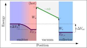
The work function is important in the theory of thermionic emission, where thermal fluctuations provide enough energy to "evaporate" electrons out of a hot material (called the 'emitter') into the vacuum. If these electrons are absorbed by another, cooler material (called the collector) then a measurable electric current will be observed. Thermionic emission can be used to measure the work function of both the hot emitter and cold collector. Generally, these measurements involve fitting to Richardson's law, and so they must be carried out in a low temperature and low current regime where space charge effects are absent.

In order to move from the hot emitter to the vacuum, an electron's energy must exceed the emitter Fermi level by an amount
determined simply by the thermionic work function of the emitter. If an electric field is applied towards the surface of the emitter, then all of the escaping electrons will be accelerated away from the emitter and absorbed into whichever material is applying the electric field. According to Richardson's law the emitted current density (per unit area of emitter), Je (A/m2), is related to the absolute temperature Te of the emitter by the equation:
where k is the Boltzmann constant and the proportionality constant Ae is the Richardson's constant of the emitter. In this case, the dependence of Je on Te can be fitted to yield We.
Work function of cold electron collector

The same setup can be used to instead measure the work function in the collector, simply by adjusting the applied voltage. If an electric field is applied away from the emitter instead, then most of the electrons coming from the emitter will simply be reflected back to the emitter. Only the highest energy electrons will have enough energy to reach the collector, and the height of the potential barrier in this case depends on the collector's work function, rather than the emitter's.
The current is still governed by Richardson's law. However, in this case the barrier height does not depend on We. The barrier height now depends on the work function of the collector, as well as any additional applied voltages:[11]
where Wc is the collector's thermionic work function, ΔVce is the applied collector–emitter voltage, and ΔVS is the Seebeck voltage in the hot emitter (the influence of ΔVS is often omitted, as it is a small contribution of order 10 mV). The resulting current density Jc through the collector (per unit of collector area) is again given by Richardson's Law, except now
where A is a Richardson-type constant that depends on the collector material but may also depend on the emitter material, and the diode geometry. In this case, the dependence of Jc on Te, or on ΔVce, can be fitted to yield Wc.
This retarding potential method is one of the simplest and oldest methods of measuring work functions, and is advantageous since the measured material (collector) is not required to survive high temperatures.
Methods based on photoemission

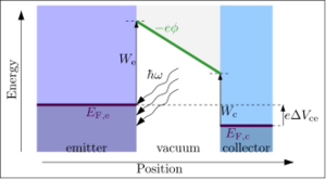
The photoelectric work function is the minimum photon energy required to liberate an electron from a substance, in the photoelectric effect. If the photon's energy is greater than the substance's work function, photoelectric emission occurs and the electron is liberated from the surface. Similar to the thermionic case described above, the liberated electrons can be extracted into a collector and produce a detectable current, if an electric field is applied into the surface of the emitter. Excess photon energy results in a liberated electron with non-zero kinetic energy. It is expected that the minimum photon energy required to liberate an electron (and generate a current) is
where We is the work function of the emitter.
Photoelectric measurements require a great deal of care, as an incorrectly designed experimental geometry can result in an erroneous measurement of work function.[9] This may be responsible for the large variation in work function values in scientific literature. Moreover, the minimum energy can be misleading in materials where there are no actual electron states at the Fermi level that are available for excitation. For example, in a semiconductor the minimum photon energy would actually correspond to the valence band edge rather than work function.[12]
Of course, the photoelectric effect may be used in the retarding mode, as with the thermionic apparatus described above. In the retarding case, the dark collector's work function is measured instead.
Kelvin probe method

The Kelvin probe technique relies on the detection of an electric field (gradient in ϕ) between a sample material and probe material. The electric field can be varied by the voltage ΔVsp that is applied to the probe relative to the sample. If the voltage is chosen such that the electric field is eliminated (the flat vacuum condition), then
Since the experimenter controls and knows ΔVsp, then finding the flat vacuum condition gives directly the work function difference between the two materials. The only question is, how to detect the flat vacuum condition? Typically, the electric field is detected by varying the distance between the sample and probe. When the distance is changed but ΔVsp is held constant, a current will flow due to the change in capacitance. This current is proportional to the vacuum electric field, and so when the electric field is neutralized no current will flow.
Although the Kelvin probe technique only measures a work function difference, it is possible to obtain an absolute work function by first calibrating the probe against a reference material (with known work function) and then using the same probe to measure a desired sample.[10] The Kelvin probe technique can be used to obtain work function maps of a surface with extremely high spatial resolution, by using a sharp tip for the probe (see Kelvin probe force microscope).
Work functions of elements
The work function depends on the configurations of atoms at the surface of the material. For example, on polycrystalline silver the work function is 4.26 eV, but on silver crystals it varies for different crystal faces as (100) face: 4.64 eV, (110) face: 4.52 eV, (111) face: 4.74 eV.[13] Ranges for typical surfaces are shown in the table below.[14]
| Ag | 4.26 – 4.74 | Al | 4.06 – 4.26 | As | 3.75 |
| Au | 5.10 – 5.47 | B | ~4.45 | Ba | 2.52 – 2.70 |
| Be | 4.98 | Bi | 4.31 | C | ~5 |
| Ca | 2.87 | Cd | 4.08 | Ce | 2.9 |
| Co | 5 | Cr | 4.5 | Cs | 1.95 |
| Cu | 4.53 – 5.10 | Eu | 2.5 | Fe | 4.67 – 4.81 |
| Ga | 4.32 | Gd | 2.90 | Hf | 3.90 |
| Hg | 4.475 | In | 4.09 | Ir | 5.00 – 5.67 |
| K | 2.29 | La | 3.5 | Li | 2.9 |
| Lu | ~3.3 | Mg | 3.66 | Mn | 4.1 |
| Mo | 4.36 – 4.95 | Na | 2.75 | Nb | 3.95 – 4.87 |
| Nd | 3.2 | Ni | 5.04 – 5.35 | Os | 5.93 |
| Pb | 4.25 | Pd | 5.22 – 5.60 | Pt | 5.12 – 5.93 |
| Rb | 2.261 | Re | 4.72 | Rh | 4.98 |
| Ru | 4.71 | Sb | 4.55 – 4.70 | Sc | 3.5 |
| Se | 5.9 | Si | 4.60 – 4.85 | Sm | 2.7 |
| Sn | 4.42 | Sr | ~2.59 | Ta | 4.00 – 4.80 |
| Tb | 3.00 | Te | 4.95 | Th | 3.4 |
| Ti | 4.33 | Tl | ~3.84 | U | 3.63 – 3.90 |
| V | 4.3 | W | 4.32 – 4.55 | Y | 3.1 |
| Yb | 2.60[15] | Zn | 3.63 – 4.9 | Zr | 4.05 |
Physical factors that determine the work function
Due to the complications described in the modelling section below, it is difficult to theoretically predict the work function with accuracy. However, various trends have been identified. The work function tends to be smaller for metals with an open lattice,[clarification needed] and larger for metals in which the atoms are closely packed. It is somewhat higher on dense crystal faces than open crystal faces, also depending on surface reconstructions for the given crystal face.
Surface dipole
The work function is not simply dependent on the "internal vacuum level" inside the material (i.e., its average electrostatic potential), because of the formation of an atomic-scale electric double layer at the surface.[7] This surface electric dipole gives a jump in the electrostatic potential between the material and the vacuum.
A variety of factors are responsible for the surface electric dipole. Even with a completely clean surface, the electrons can spread slightly into the vacuum, leaving behind a slightly positively charged layer of material. This primarily occurs in metals, where the bound electrons do not encounter a hard wall potential at the surface but rather a gradual ramping potential due to image charge attraction. The amount of surface dipole depends on the detailed layout of the atoms at the surface of the material, leading to the variation in work function for different crystal faces.
Doping and electric field effect (semiconductors)

In a semiconductor, the work function is sensitive to the doping level at the surface of the semiconductor. Since the doping near the surface can also be controlled by electric fields, the work function of a semiconductor is also sensitive to the electric field in the vacuum.
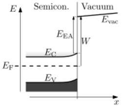
The reason for the dependence is that, typically, the vacuum level and the conduction band edge retain a fixed spacing independent of doping. This spacing is called the electron affinity (note that this has a different meaning than the electron affinity of chemistry); in silicon for example the electron affinity is 4.05 eV.[16] If the electron affinity EEA and the surface's band-referenced Fermi level EF-EC are known, then the work function is given by
where EC is taken at the surface.
From this one might expect that by doping the bulk of the semiconductor, the work function can be tuned. In reality, however, the energies of the bands near the surface are often pinned to the Fermi level, due to the influence of surface states.[17] If there is a large density of surface states, then the work function of the semiconductor will show a very weak dependence on doping or electric field.[18]
Theoretical models of metal work functions
Theoretical modeling of the work function is difficult, as an accurate model requires a careful treatment of both electronic many body effects and surface chemistry; both of these topics are already complex in their own right.
One of the earliest successful models for metal work function trends was the jellium model,[19] which allowed for oscillations in electronic density nearby the abrupt surface (these are similar to Friedel oscillations) as well as the tail of electron density extending outside the surface. This model showed why the density of conduction electrons (as represented by the Wigner–Seitz radius rs) is an important parameter in determining work function.
The jellium model is only a partial explanation, as its predictions still show significant deviation from real work functions. More recent models have focused on including more accurate forms of electron exchange and correlation effects, as well as including the crystal face dependence (this requires the inclusion of the actual atomic lattice, something that is neglected in the jellium model).[7][20]
Temperature dependence of the electron work function
The electron behavior in metals varies with temperature and is largely reflected by the electron work function. A theoretical model for predicting the temperature dependence of the electron work function, developed by Rahemi et al.[21] explains the underlying mechanism and predicts this temperature dependence for various crystal structures via calculable and measurable parameters. In general, as the temperature increases, the EWF decreases via and is a calculable material property which is dependent on the crystal structure (for example, BCC, FCC). is the electron work function at T=0 and is constant throughout the change.
References
- ↑ 1.0 1.1 Kittel, Charles (1996). Introduction to Solid State Physics (7th ed.). Wiley.
- ↑ Gersten, Joel (2001). The physics and chemistry of materials. New York: Wiley. ISBN 978-0-471-05794-9. OCLC 46538642.
- ↑ Herbert Kroemer, "Quasi-Electric Fields and Band Offsets: Teaching Electrons New Tricks" Nobel lecture
- ↑ "Barrier Height Correlations and Systematics". http://academic.brooklyn.cuny.edu/physics/tung/Schottky/systematics.htm.
- ↑ Behunin, R. O.; Intravaia, F.; Dalvit, D. A. R.; Neto, P. A. M.; Reynaud, S. (2012). "Modeling electrostatic patch effects in Casimir force measurements". Physical Review A 85 (1). doi:10.1103/PhysRevA.85.012504. Bibcode: 2012PhRvA..85a2504B.
- ↑ Will, C. M. (2011). "Finally, results from Gravity Probe B". Physics 4 (43). doi:10.1103/Physics.4.43. Bibcode: 2011PhyOJ...4...43W.
- ↑ 7.0 7.1 7.2 "Metal surfaces 1a". http://venables.asu.edu/qmms/PROJ/metal1a.html.
- ↑ Thomas Iii, S. W.; Vella, S. J.; Dickey, M. D.; Kaufman, G. K.; Whitesides, G. M. (2009). "Controlling the Kinetics of Contact Electrification with Patterned Surfaces". Journal of the American Chemical Society 131 (25): 8746–8747. doi:10.1021/ja902862b. PMID 19499916. Bibcode: 2009JAChS.131.8746T.
- ↑ 9.0 9.1 Helander, M. G.; Greiner, M. T.; Wang, Z. B.; Lu, Z. H. (2010). "Pitfalls in measuring work function using photoelectron spectroscopy". Applied Surface Science 256 (8): 2602. doi:10.1016/j.apsusc.2009.11.002. Bibcode: 2010ApSS..256.2602H.
- ↑ 10.0 10.1 Fernández Garrillo, P. A.; Grévin, B.; Chevalier, N.; Borowik, Ł. (2018). "Calibrated work function mapping by Kelvin probe force microscopy". Review of Scientific Instruments 89 (4): 043702. doi:10.1063/1.5007619. PMID 29716375. Bibcode: 2018RScI...89d3702F. https://hal.archives-ouvertes.fr/hal-02277068/file/Garrillo_2018_1.5007619.pdf.
- ↑ G.L. Kulcinski, "Thermionic Energy Conversion" [1]
- ↑ "Photoelectron Emission". http://www.virginia.edu/ep/SurfaceScience/PEE.html.
- ↑ Dweydari, A. W.; Mee, C. H. B. (1975). "Work function measurements on (100) and (110) surfaces of silver". Physica Status Solidi A 27 (1): 223. doi:10.1002/pssa.2210270126. Bibcode: 1975PSSAR..27..223D.
- ↑ CRC Handbook of Chemistry and Physics version 2008, p. 12–124.
- ↑ Nikolic, M. V.; Radic, S. M.; Minic, V.; Ristic, M. M. (February 1996). "The dependence of the work function of rare earth metals on their electron structure". Microelectronics Journal 27 (1): 93–96. doi:10.1016/0026-2692(95)00097-6. ISSN 0026-2692.
- ↑ Virginia Semiconductor (June 2002). "The General Properties of Si, Ge, SiGe, SiO2 and Si3N4". http://www.virginiasemi.com/pdf/generalpropertiessi62002.pdf.
- ↑ "Semiconductor Free Surfaces". http://academic.brooklyn.cuny.edu/physics/tung/Schottky/surface.htm.
- ↑ Bardeen, J. (1947). "Surface States and Rectification at a Metal Semi-Conductor Contact". Physical Review 71 (10): 717–727. doi:10.1103/PhysRev.71.717. Bibcode: 1947PhRv...71..717B.
- ↑ Lang, N.; Kohn, W. (1971). "Theory of Metal Surfaces: Work Function". Physical Review B 3 (4): 1215. doi:10.1103/PhysRevB.3.1215. Bibcode: 1971PhRvB...3.1215L.
- ↑ Kiejna, A.; Wojciechowski, K.F. (1996). Metal Surface Electron Physics. Elsevier. ISBN 978-0-08-053634-7.
- ↑ Rahemi, Reza; Li, Dongyang (April 2015). "Variation in electron work function with temperature and its effect on Young's modulus of metals". Scripta Materialia 99 (2015): 41–44. doi:10.1016/j.scriptamat.2014.11.022.
Further reading
- Ashcroft; Mermin (1976). Solid State Physics. Thomson Learning, Inc..
- Goldstein, Newbury (2003). Scanning Electron Microscopy and X-Ray Microanalysis. New York: Springer.
For a quick reference to values of work function of the elements:
- Michaelson, Herbert B. (1977). "The work function of the elements and its periodicity". J. Appl. Phys. 48 (11): 4729. doi:10.1063/1.323539. Bibcode: 1977JAP....48.4729M.
External links
- Work function of polymeric insulators (Table 2.1)
- Work function of diamond and doped carbon
- Work functions of common metals
- Work functions of various metals for the photoelectric effect
- Physics of free surfaces of semiconductors
 |
 KSF
KSF