Haswell (Microarchitecture)
 From Handwiki
 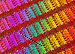 A Haswell wafer with several dies, with a pin for scale | |
| General Info | |
|---|---|
| Launched | June 4, 2013 |
| Marketed by | Intel |
| Designed by | Intel |
| Common manufacturer(s) |
|
| CPUID code | 0306C3h |
| Product code |
|
| Performance | |
| Max. CPU clock rate | 800 MHz to 4.4 GHz |
| QPI speeds | 9.6 GT/s |
| DMI speeds | 4 GT/s |
| Cache | |
| L1 cache | 64 KB per core (32 KB instructions + 32 KB data) |
| L2 cache | 256 KB per core |
| L3 cache | 2–45 MB (shared) |
| L4 cache | 128 MB of eDRAM (Iris Pro models only) |
| Architecture and classification | |
| Min. feature size | 22 nm (Tri-Gate) |
| Microarchitecture | Haswell |
| Instruction set | x86-64 |
| Instructions | x86, x86-64 |
| Extensions |
|
| Physical specifications | |
| Cores |
|
| GPU(s) |
|
| Socket(s) |
|
| Products, models, variants | |
| Model(s) |
|
| Brand name(s) |
|
| History | |
| Predecessor | Sandy Bridge (Tock) Ivy Bridge (Tick) |
| Successor | Broadwell (Tick/Process) Skylake (Tock) |
Haswell is the codename for a processor microarchitecture developed by Intel as the "fourth-generation core" successor to the Ivy Bridge (which is a die shrink/tick of the Sandy Bridge microarchitecture).[1] Intel officially announced CPUs based on this microarchitecture on June 4, 2013, at Computex Taipei 2013,[2] while a working Haswell chip was demonstrated at the 2011 Intel Developer Forum.[3] With Haswell, which uses a 22 nm process,[4] Intel also introduced low-power processors designed for convertible or "hybrid" ultrabooks, designated by the "U" suffix.
Haswell CPUs are used in conjunction with the Intel 8 Series chipsets, Intel 9 Series chipsets, and Intel C220 series chipsets.
At least one Haswell-based processor was still being sold in 2022 — the Pentium G3420.[5][6] Windows 7 through Windows 10 were released for the Haswell microarchitecture.
Design
The Haswell architecture is specifically designed[7] to optimize the power savings and performance benefits from the move to FinFET (non-planar, "3D") transistors on the improved 22 nm process node.[8]
Haswell has been launched in three major forms:[9]
- Desktop version (LGA 1150 socket and the LGA 2011-v3 socket): Haswell-DT
- Mobile/Laptop version (PGA socket): Haswell-MB
- BGA version:
- 47 W and 57 W TDP classes: Haswell-H (for "All-in-one" systems, Mini-ITX form factor motherboards, and other small footprint formats)
- 13.5 W and 15 W TDP classes (MCP): Haswell-ULT (for Intel's UltraBook platform)
- 10 W TDP class (SoC): Haswell-ULX (for tablets and certain UltraBook-class implementations)
Notes
- ULT = Ultra Low TDP; ULX = Ultra Low eXtreme TDP
- Only certain quad-core variants and BGA R-series stock keeping units (SKUs) receive GT3e (Intel Iris Pro 5200) integrated graphics. All other models have GT3 (Intel HD 5000 or Intel Iris 5100), GT2 (Intel HD 4200, 4400, 4600, P4600 or P4700) or GT1 (Intel HD Graphics) integrated graphics.[10] See also Intel HD and Iris Graphics for more details.
- Due to the low power requirements of tablet and UltraBook platforms, Haswell-ULT and Haswell-ULX are only available in dual-core configurations. All other versions come as dual- or quad-core variants.
Performance
Compared to Ivy Bridge:
- Approximately 8% faster vector processing[11]
- Up to 5% higher single-threaded performance
- 6% higher multi-threaded performance
- Desktop variants of Haswell draw between 8% and 23% more power under load than Ivy Bridge.[11][12][13]
- A 6% increase in sequential CPU performance (eight execution ports per core versus six)[11]
- Up to 20% performance increase over the integrated HD4000 GPU (Haswell HD4600 vs Ivy Bridge's built-in Intel HD4000)[11]
- Total performance improvement on average is about 3%[11]
- Around 15 °C hotter than Ivy Bridge, while clock frequencies of over 4.6 GHz are achievable[14][15][16][17][18][19]
Technology
Features carried over from Ivy Bridge
- 22 nm manufacturing process[4]
- 3D Tri-Gate FinFET transistors[20]
- Micro-operation cache (Uop Cache) capable of storing 1.5 K micro-operations (approximately 6 KB in size)[21]
- 14- to 19-stage instruction pipeline, depending on the micro-operation cache hit or miss (an approach used in the even earlier Sandy Bridge microarchitecture)[21]
- Improve OoO window from 168 to 192[22]
- Queue Allocation from 28/threads to 56
- Mainstream variants are up to quad-core.[23]
- Native support for dual-channel DDR3/DDR3L memory,[24] with up to 32 GB of RAM on LGA 1150 variants
- 64 KB (32 KB Instruction + 32 KB Data) L1 cache and 256 KB L2 cache per core[25]
- A total of 16 PCI Express 3.0 lanes on LGA 1150 variants[26]
New features
CPU
- Wider core:[27] fourth arithmetic logic unit (ALU), third address generation unit (AGU),[28][29][30] second branch execution unit (BEU), deeper buffers, higher cache bandwidth, improved front-end and memory controller, higher load/store bandwidth.
- New instructions[31] (HNI, includes Advanced Vector Extensions 2 (AVX2), gather, BMI1, BMI2, ABM and FMA3 support).[32]
- The instruction decode queue, which holds instructions after they have been decoded, is no longer statically partitioned between the two threads that each core can service.[21]
- Intel Transactional Synchronization Extensions (TSX) for the Haswell-EX variant. In August 2014 Intel announced that a bug exists in the TSX implementation on the current steppings of Haswell, Haswell-E, Haswell-EP and early Broadwell CPUs, which resulted in disabling the TSX feature on affected CPUs via a microcode update.[33][34][35][36]
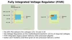
- Fully integrated voltage regulator (FIVR), thereby moving some of the components from motherboard onto the CPU.[37][38][39]
- New advanced power-saving system; due to Haswell's new low-power C6 and C7 sleep states, not all power supply units (PSUs) are suitable for computers with Haswell CPUs.[40][41]
- 37, 47, 57 W thermal design power (TDP) mobile processors.[23]
- 35, 45, 65, 84, 88, 95 and 130–140 W (high-end, Haswell-E) TDP desktop processors.[23]
- 15 W or 11.5W TDP processors for the Ultrabook platform (multi-chip package like Westmere)[42] leading to reduced heat, which results in thinner as well as lighter Ultrabooks, but the performance level is slightly lower than the 17 W version.[43]
Translation lookaside buffer sizes[44][45] Cache Page size Name Level 4 KB 2 MB 1 GB DTLB 1st 64 32 4 ITLB 1st 128 8 / logical core none STLB 2nd 1024 none
GPU
- Hardware graphics support for Direct3D 11.1 and OpenGL 4.3.[46][47][48] Intel 10.18.14.5180 driver is the last planned driver release on Windows 7/8.1.[49]
- Four versions of the integrated GPU: GT1, GT2, GT3 and GT3e, where GT3 version has 40 execution units (EUs). Haswell's predecessor, Ivy Bridge, has a maximum of 16 EUs. GT3e version with 40 EUs and on-package 128 MB of embedded DRAM (eDRAM), called Crystalwell, is available only in mobile H-SKUs and desktop (BGA-only) R-SKUs. Effectively, this eDRAM is a Level 4 cache; it is shared dynamically between the on-die GPU and CPU, and serving as a victim cache to the CPU's Level 3 cache.[50][51][52][53][54]
I/O
- New sockets and chipsets:
- LGA 1150 for desktops, and rPGA947 and BGA1364 for the mobile market.[55]
- Z97 (performance) and H97 (mainstream) chipsets for the Haswell Refresh and Broadwell, in Q2 2014.[56]
- LGA 2011-v3 with X99 chipset for the enthusiast-class desktop platform Haswell-E.[57]
- DDR4 for enterprise/server segments[58] and for the Enthusiast-Class Desktop Platform Haswell-E[59]
- Variable Base clock (BClk)[60] like LGA 2011.[61]
- Optional support for Thunderbolt technology and Thunderbolt 2.0[62][63]
- Shrink of the Platform Controller Hub (PCH), from 65 nm to 32 nm.[64]
Server processors features
- Haswell-EP variant, released in September 2014, with up to 18 cores and marketed as the Xeon E5-1600 v3 and Xeon E5-2600 v3 series.[65]
- Haswell-EX variant, released in May 2015, with 18 cores and functioning TSX.[35][66][67]
- A new cache design.
- Up to 35 MB total unified cache (last level cache, LLC) for Haswell-EP[68] and up to 40 MB for Haswell-EX.
- LGA 2011-v3 socket replaces LGA 2011 for the Haswell EP; the new socket has the same number of pins, but it is keyed differently due to electrical incompatibility.[69][70][71]
- The already launched Xeon E3 v3 Haswells will get a refresh in spring 2014,[72] together with a refreshed Intel C220 series PCH chipset.[73]
- TDP up to 160 W for Haswell-EP.[74]
- Haswell-EP models with ten and more cores support cluster on die (COD) operation mode,[75] allowing CPU's multiple columns of cores and last level cache (LLC) slices to be logically divided into what is presented as two non-uniform memory access (NUMA) CPUs to the operating system. By keeping data and instructions local to the "partition" of CPU which is processing them, therefore decreasing the LLC access latency, COD brings performance improvements to NUMA-aware operating systems and applications.[76]
Haswell Refresh
Around the middle of 2014, Intel released a refresh of Haswell, simply titled Haswell Refresh. When compared to the original Haswell CPUs lineup, Haswell Refresh CPUs offer a modest increase in clock frequencies, usually of 100 MHz.[77] Haswell Refresh CPUs are supported by Intel's 9 Series chipsets (Z97 and H97, codenamed Wildcat Point), while motherboards with 8 Series chipsets (codenamed Lynx Point) usually require a BIOS update to support Haswell Refresh CPUs.[78]
The CPUs codenamed Devil's Canyon, covering the i5 and i7 K-series SKUs, employ a new and improved thermal interface material (TIM) called next-generation polymer thermal interface material (NGPTIM). This improved TIM reduces the CPU's operating temperatures and improves the overclocking potential, as something that had been problematic since the introduction of Ivy Bridge.[79] Other changes for the Devil's Canyon CPUs include a TDP increase to 88 W, additional decoupling capacitors to help smooth out the outputs from the fully integrated voltage regulator (FIVR), and support for the VT-d that was previously limited to non-K-series SKUs.[80] TSX was another feature brought over from the non-K-series SKUs, until August 2014 when a microcode update disabled TSX due to a bug that was discovered in its implementation.[35][36]
Windows XP and Vista support
While Ivy Bridge is the last Intel processor to fully support all versions of Windows XP, Haswell includes limited driver support for certain XP editions such as POSReady2009. People have modified the graphics driver for these versions to adapt to normal Windows XP to varying degrees of success.
Windows Vista support is also dropped with this processor as well. People who have installed x64 version of Vista have reported various problems such as services not starting automatically. The KB4493471 update (officially intended only for Windows Server 2008, but can be installed on Vista) contains a HAL driver that allegedly fixes these issues; however, upon several tests it's been confirmed - it doesn't fix any of the issues. Windows XP and earlier, and all x86 versions and editions of Vista are unaffected by this bug.[citation needed]
List of Haswell processors
Desktop processors
- All models support: MMX, SSE, SSE2, SSE3, SSSE3, SSE4.1, SSE4.2, F16C, Enhanced Intel SpeedStep Technology (EIST), Intel 64, XD bit (an NX bit implementation), Intel VT-x, and Smart Cache.
- Core i3, i5 and i7 support AVX, AVX2, BMI1, BMI2, FMA3, and AES-NI.[81]
- Core i3 and i7, as well as the Core i5-4570T and i5-4570TE, support Hyper-Threading (HT).[81]
- Core i5 and i7 support Turbo Boost 2.0.[81]
- Although it was initially supported on selected models, since August 2014 desktop variants no longer support TSX due to a bug that was discovered in its implementation; as a workaround, a microcode update disabled the TSX feature.[33][35][36][81]
- SKUs below 45xx as well as R-series and K-series SKUs do not support Trusted Execution Technology or vPro.[81]
- Intel VT-d, which is Intel's IOMMU, is supported on all i5 and i7 SKUs except the i5-4670K and i7-4770K.[81][82][83] Support for VT-d requires the chipset and motherboard to also support VT-d.
- Models i5-4690K and i7-4790K, codenamed Devil's Canyon, have a better internal thermal grease to help heat escape and an improved internal voltage regulator ("FIVR"), to help deliver cleaner power in situations like overclocking.
- Transistors: 1.4 billion[84][85]
- Die size: 177 mm2[84]
- Intel HD and Iris Graphics in following variants:
- R-series desktop processors feature Intel Iris Pro 5200 graphics (GT3e).[86]
- The i3-41xxx processors include HD 4400 graphics (GT2).
- All other i3, i5 and i7 desktop processors include Intel HD 4600 graphics (GT2).[87]
- Celeron and Pentium processors contain Intel HD Graphics (GT1).
- Pentium G3258, also known as the Pentium Anniversary Edition, has an unlocked multiplier. Its release marks 20 years of "Pentium" as a brand.[88]
The following table lists available desktop processors.
| Target segment |
Cores (threads) |
Processor branding and model |
GPU model | CPU clock rate | Graphics clock rate | Cache | TDP | PCIe 3.0 lane configurations[a] |
VT-d[b] | Release date |
Release price (USD) |
Motherboard | ||||||
|---|---|---|---|---|---|---|---|---|---|---|---|---|---|---|---|---|---|---|
| Normal | Turbo | Normal | Turbo | L3 | L4[lower-alpha 1] | Socket | Interface | Memory | ||||||||||
| Enthusiast / High-End | 8 (16) | Core i7 Extreme |
5960X | N/A | 3.0 GHz | 3.5 GHz | N/A | N/A | 20 MB | N/A | 140 W | 2×16 + 1×8 | Yes | August 29, 2014[89] | $999 | LGA 2011-v3 | DMI 2.0 PCIe 3.0 |
Up to quad channel DDR4-2133 |
| 6 (12) | 5930K | 3.5 GHz | 3.7 GHz | 15 MB | $583 | |||||||||||||
| 5820K | 3.3 GHz | 3.6 GHz | 1×16 + 1×8 + 1×4 | $389 | ||||||||||||||
| Performance | 4 (8) | Core i7 | 4790K | HD 4600 (GT2) |
4.0 GHz | 4.4 GHz | 350 MHz[90] | 1.25 GHz | 8 MB | 88 W | 1×16 2×8 1×8 + 2×4 |
June 2, 2014 | $339 | LGA 1150 |
Up to dual channel DDR3-1600[91] | |||
| 4790 | 3.6 GHz | 4.0 GHz | 1.2 GHz | 84 W | May 11, 2014 | $303 | ||||||||||||
| 4790S | 3.2 GHz | 65 W | ||||||||||||||||
| 4790T | 2.7 GHz | 3.9 GHz | 45 W | |||||||||||||||
| 4785T | 2.2 GHz | 3.2 GHz | 35 W | |||||||||||||||
| 4771 | 3.5 GHz | 3.9 GHz | 84 W | September 1, 2013 | $320 | |||||||||||||
| 4770K | 1.25 GHz | No | June 2, 2013[92] | $339 | ||||||||||||||
| 4770 | 3.4 GHz | 1.2 GHz | Yes | $303 | ||||||||||||||
| 4770S | 3.1 GHz | 65 W | ||||||||||||||||
| 4770R | Iris Pro 5200 (GT3e) |
3.2 GHz | 200 MHz | 1.3 GHz | 6 MB | 128 MB | $392 | BGA 1364 | ||||||||||
| 4770T | HD 4600 (GT2) |
2.5 GHz | 3.7 GHz | 350 MHz[90] | 1.2 GHz | 8 MB | N/A | 45 W | $303 | LGA 1150 | ||||||||
| 4770TE | 2.3 GHz | 3.3 GHz | 1 GHz | |||||||||||||||
| 4765T | 2.0 GHz | 3.0 GHz | 1.2 GHz | 35 W | ||||||||||||||
| Mainstream | 4 (4) | Core i5 | 4690K | 3.5 GHz | 3.9 GHz | 6 MB | 88 W | June 2, 2014 | $242 | |||||||||
| 4690 | 84 W | May 11, 2014 | $213 | |||||||||||||||
| 4690S | 3.2 GHz | 65 W | ||||||||||||||||
| 4690T | 2.5 GHz | 3.5 GHz | 45 W | |||||||||||||||
| 4670K | 3.4 GHz | 3.8 GHz | 84 W | No | June 2, 2013 | $242 | ||||||||||||
| 4670 | Yes | $213 | ||||||||||||||||
| 4670S | 3.1 GHz | 65 W | ||||||||||||||||
| 4670R | Iris Pro 5200 (GT3e) |
3.0 GHz | 3.7 GHz | 200 MHz | 1.3 GHz | 4 MB | 128 MB | $310 | BGA 1364 | |||||||||
| 4670T | HD 4600 (GT2) |
2.3 GHz | 3.3 GHz | 350 MHz[90] | 1.2 GHz | 6 MB | N/A | 45 W | $213 | LGA 1150 | ||||||||
| 4590 | 3.3 GHz | 3.7 GHz | 1.15 GHz | 84 W | May 11, 2014 | $192 | ||||||||||||
| 4590S | 3.0 GHz | 65 W | ||||||||||||||||
| 4590T | 2.0 GHz | 3.0 GHz | 35 W | |||||||||||||||
| 4570 | 3.2 GHz | 3.6 GHz | 84 W | June 2, 2013 | ||||||||||||||
| 4570S | 2.9 GHz | 65 W | ||||||||||||||||
| 4570R | Iris Pro 5200 (GT3e) |
2.7 GHz | 3.2 GHz | 200 MHz | 4 MB | 128 MB | $288 | BGA 1364 | ||||||||||
| 2 (4) | 4570T | HD 4600 (GT2) |
2.9 GHz | 3.6 GHz | N/A | 35 W | $192 | LGA 1150 | ||||||||||
| 4570TE | 2.7 GHz | 3.3 GHz | 350 MHz[90] | 1 GHz | ||||||||||||||
| 4 (4) | 4460 | 3.2 GHz | 3.4 GHz | 1.1 GHz | 6 MB | 84 W | May 11, 2014 | $182 | ||||||||||
| 4460S | 2.9 GHz | 65 W | ||||||||||||||||
| 4460T | 1.9 GHz | 2.7 GHz | 35 W | |||||||||||||||
| 4440 | 3.1 GHz | 3.3 GHz | 84 W | September 1, 2013 | ||||||||||||||
| 4440S | 2.8 GHz | 65 W | ||||||||||||||||
| 4430 | 3.0 GHz | 3.2 GHz | 84 W | June 2, 2013[92] | ||||||||||||||
| 4430S | 2.7 GHz | 65 W | ||||||||||||||||
| 2 (4) | Core i3 | 4370 | 3.8 GHz | N/A | 1.15 GHz | 4 MB | 54 W | No | July 20, 2014 | $149 | ||||||||
| 4360 | 3.7 GHz | May 11, 2014 | ||||||||||||||||
| 4350 | 3.6 GHz | $138 | ||||||||||||||||
| 4340 | September 1, 2013 | $149 | ||||||||||||||||
| 4330 | 3.5 GHz | $138 | ||||||||||||||||
| 4370T | 3.3 GHz | 200 MHz | 35 W | March 30, 2015 | ||||||||||||||
| 4360T | 3.2 GHz | July 20, 2014 | ||||||||||||||||
| 4350T | 3.1 GHz | May 11, 2014 | ||||||||||||||||
| 4330T | 3.0 GHz | September 1, 2013 | ||||||||||||||||
| 4340TE | 2.6 GHz | 350 MHz | 1 GHz | May 11, 2014 | $138 | |||||||||||||
| 4330TE | 2.4 GHz | September 1, 2013 | $122 | |||||||||||||||
| 4170 | HD 4400 (GT2) |
3.7 GHz | 1.15 GHz | 3 MB | 54 W | March 30, 2015 | $117 | |||||||||||
| 4160 | 3.6 GHz | July 20, 2014 | ||||||||||||||||
| 4150 | 3.5 GHz | May 11, 2014 | ||||||||||||||||
| 4130 | 3.4 GHz | September 1, 2013 | $122 | |||||||||||||||
| 4170T | 3.2 GHz | 200 MHz | 35 W | March 30, 2015 | $117 | |||||||||||||
| 4160T | 3.1 GHz | July 20, 2014 | ||||||||||||||||
| 4150T | 3.0 GHz | May 11, 2014 | ||||||||||||||||
| 4130T | 2.9 GHz | September 1, 2013 | $122 | |||||||||||||||
| Budget | 2 (2) | Pentium | G3470 | HD Graphics | 3.6 GHz | 350 MHz | 1.1 GHz | 53 W | March 30, 2015 | $86 | ||||||||
| G3460 | 3.5 GHz | July 20, 2014 | ||||||||||||||||
| G3450 | 3.4 GHz | May 11, 2014 | ||||||||||||||||
| G3440 | 3.3 GHz | $75 | ||||||||||||||||
| G3430 | December 1, 2013 | $86 | ||||||||||||||||
| G3420 | 3.2 GHz | $75 | ||||||||||||||||
| G3460T | 3.0 GHz | 200 MHz | 1.1 GHz | 35 W | March 30, 2015 | |||||||||||||
| G3450T | 2.9 GHz | July 20, 2014 | ||||||||||||||||
| G3440T | 2.8 GHz | May 11, 2014 | ||||||||||||||||
| G3420T | 2.7 GHz | December 1, 2013 | ||||||||||||||||
| G3320TE | 2.3 GHz | 350 MHz | 1 GHz | Up to dual channel DDR3-1333 | ||||||||||||||
| G3260 | 3.3 GHz | 1.1 GHz | 53 W | March 30, 2015 | $64 | |||||||||||||
| G3258[c] | 3.2 GHz | June 2, 2014 | $72 | |||||||||||||||
| G3250 | July 20, 2014 | $64 | ||||||||||||||||
| G3240 | 3.1 GHz | May 11, 2014 | ||||||||||||||||
| G3220 | 3.0 GHz | December 1, 2013 | ||||||||||||||||
| G3260T | 2.9 GHz | 200 MHz | 35 W | March 30, 2015 | ||||||||||||||
| G3250T | 2.8 GHz | July 20, 2014 | ||||||||||||||||
| G3240T | 2.7 GHz | May 11, 2014 | ||||||||||||||||
| G3220T | 2.6 GHz | December 1, 2013 | ||||||||||||||||
| Celeron | G1850 | 2.9 GHz | 350 MHz | 1.05 GHz | 2 MB | 53 W | May 11, 2014 | $52 | ||||||||||
| G1840 | 2.8 GHz | $42 | ||||||||||||||||
| G1830 | December 1, 2013 | $52 | ||||||||||||||||
| G1820 | 2.7 GHz | $42 | ||||||||||||||||
| G1840T | 2.5 GHz | 200 MHz | 35 W | May 11, 2014 | ||||||||||||||
| G1820T | 2.4 GHz | December 1, 2013 | ||||||||||||||||
| G1820TE | 2.2 GHz | 1 GHz | ||||||||||||||||
- a Some of these configurations could be disabled by the chipset. For example, H-series chipsets disable all PCIe 3.0 lane configurations except 1×16.
- b This feature also requires a chipset that supports VT-d like the Q87 chipset or the X99 chipset.
- c This is called 20th Anniversary Edition and has an unlocked multiplier.
SKU suffixes to denote:
- K – unlocked (adjustable CPU multiplier up to 63x)
- The Pentium G3258 CPU is unlocked despite not having the K-suffix.
- S – performance-optimized lifestyle (low power with 65 W TDP)
- T – power-optimized lifestyle (ultra low power with 35–45 W TDP)
- R – BGA packaging / High-performance GPU (currently Iris Pro 5200 (GT3e))
- X – extreme edition (adjustable CPU ratio with no ratio limit)
Server processors


- All models support: MMX, SSE, SSE2, SSE3, SSSE3, SSE4.1, SSE4.2, AVX (Advanced Vector Extensions), AVX2, FMA3, F16C, BMI (Bit Manipulation Instructions 1)+BMI2, Enhanced Intel SpeedStep Technology (EIST), Intel 64, XD bit (an NX bit implementation), TXT, Intel vPro, Intel VT-x, Intel VT-d, hyper-threading (except E3-1220 v3 and E3-1225 v3), Turbo Boost 2.0, AES-NI, and Smart Cache.
- Haswell-EX models (E7-48xx/88xx v3) support TSX, while for Haswell-E, Haswell-WS (E3-12xx v3) and Haswell-EP (E5-16xx/26xx v3) models it was disabled via a microcode update in August 2014, due to a bug that was discovered in the TSX implementation.[35][36]
- Transistors: 5.56 billion[93]
- Die size: 661 mm2[93]
The first digit of the model number designates the largest supported multi-socket configuration; thus, E5-26xx v3 models support up to dual-socket configurations, while the E7-48xx v3 and E7-88xx v3 models support up to quad- and eight-socket configurations, respectively. Also, E5-16xx/26xx v3 and E7-48xx/88xx v3 models have no integrated GPU.
Lists of launched server processors are below, split between Haswell E3-12xx v3, E5-16xx/26xx v3 and E7-48xx/88xx v3 models.
| Target segment |
Cores (threads) |
Processor branding and model |
CPU clock rate | L3 cache |
TDP | Release date |
Release price (USD) |
Motherboard | ||||
|---|---|---|---|---|---|---|---|---|---|---|---|---|
| Normal | Turbo | Socket | Interface | Memory | ||||||||
| Server | 4 (8) | Xeon E7 v3 | E7-8893v3 | 3.2 GHz | 3.5 GHz | 45 MB | 140 W | May 2015 | $6,841 | LGA 2011-1 |
QPI (up to 9.6 GT/s[lower-alpha 2]) DMI 2.0 PCIe 3.0 |
Up to DDR4-1866 or DDR3-1600 |
| 10 (20) | E7-8891v3 | 2.8 GHz | 165 W | |||||||||
| 18 (36) | E7-8890v3 | 2.5 GHz | 3.3 GHz | $7,174 | ||||||||
| E7-8880v3 | 2.3 GHz | 3.1 GHz | 150 W | $5,895 | ||||||||
| E7-8880Lv3 | 2.0 GHz | 2.8 GHz | 115 W | $6,063 | ||||||||
| E7-8870v3 | 2.1 GHz | 2.9 GHz | 140 W | $4,672 | ||||||||
| 16 (32) | E7-8867v3 | 2.5 GHz | 3.3 GHz | 165 W | ||||||||
| E7-8860v3 | 2.2 GHz | 3.2 GHz | 40 MB | $4,061 | ||||||||
| 14 (28) | E7-4850v3 | 2.8 GHz | 35 MB | 115 W | $3,003 | |||||||
| 12 (24) | E7-4830v3 | 2.1 GHz | 2.7 GHz | 30 MB | $2,170 | |||||||
| 10 (20) | E7-4820v3 | 1.9 GHz | N/A | 25 MB | $1,502 | |||||||
| 8 (16) | E7-4809v3 | 2.0 GHz | ||||||||||
| Target segment |
Cores (threads) |
Processor branding and model |
CPU clock rate | CPU AVX clock rate[96] |
L3 cache |
TDP | Release date |
Release price (USD) tray / box |
Motherboard | |||||
|---|---|---|---|---|---|---|---|---|---|---|---|---|---|---|
| Normal | Turbo | Normal | Turbo | Socket | Interface | Memory | ||||||||
| Server | 18 (36) | Xeon E5 v3 | 2699v3 | 2.3 GHz | 3.6 GHz | 1.9 GHz | 3.3 GHz | 45 MB | 145 W | September 9, 2014 | N/A | LGA 2011-3 |
QPI (up to 9.6 GT/s[lower-alpha 2]) DMI 2.0 PCIe 3.0 |
up to DDR4-2133 |
| 16 (32) | 2698v3 | 40 MB | 135 W | |||||||||||
| 2698Av3[97] | 2.8 GHz | 3.2 GHz | 2.3 GHz | 2.9 GHz | 165 W | November 2014 | OEM | |||||||
| 14 (28) | 2697v3 | 2.6 GHz | 3.6 GHz | 2.2 GHz | 3.3 GHz | 35 MB | 145 W | September 9, 2014 | $2,702 / $2,706 | |||||
| 2695v3 | 2.3 GHz | 3.3 GHz | 1.9 GHz | 3.0 GHz | 120 W | $2,424 / $2,428 | ||||||||
| 12 (24) | 2690v3 | 2.6 GHz | 3.5 GHz | 2.3 GHz | 3.2 GHz | 30 MB | 135 W | $2,090 / $2,094 | ||||||
| 14 (28) | 2683v3 | 2.0 GHz | 3.0 GHz | 1.7 GHz | 2.7 GHz | 35 MB | 120 W | $1,846 / — | ||||||
| 12 (24) | 2680v3 | 2.5 GHz | 3.3 GHz | 2.1 GHz | 3.1 GHz | 30 MB | $1,745 / $1,749 | |||||||
| 2673v3[lower-alpha 3] | 2.4 GHz | 3.1 GHz | 105 W | |||||||||||
| 2670v3 | 2.3 GHz | 3.1 GHz | 2.0 GHz | 2.9 GHz | 120 W | $1,589 / $1,593 | ||||||||
| 8 (16) | 2667v3 | 3.2 GHz | 3.6 GHz | 2.7 GHz | 3.5 GHz | 20 MB | 135 W | $2,057 / — | ||||||
| 10 (20) | 2660v3 | 2.6 GHz | 3.3 GHz | 2.2 GHz | 3.1 GHz | 25 MB | 105 W | $1,445 / $1,449 | ||||||
| 12 (24) | 2650Lv3 | 1.8 GHz | 2.5 GHz | 1.5 GHz | 2.3 GHz | 30 MB | 65 W | $1,329 / — | ||||||
| 2658v3 | 2.2 GHz | 2.9 GHz | 1.9 GHz | 3.0 GHz | 105 W | $1,832 / — | ||||||||
| 10 (20) | 2650v3 | 2.3 GHz | 3.0 GHz | 2.0 GHz | 2.8 GHz | 25 MB | $1,166 / $1,171 | |||||||
| 12 (24) | 2648Lv3 | 1.8 GHz | 2.5 GHz | 1.5 GHz | 2.2 GHz | 30 MB | 75 W | $1,544 / — | ||||||
| 6 (12) | 2643v3 | 3.4 GHz | 3.7 GHz | 2.8 GHz | 3.6 GHz | 20 MB | 135 W | $1,552 / — | ||||||
| 8 (16) | 2640v3 | 2.6 GHz | 3.4 GHz | 2.2 GHz | 3.4 GHz | 20 MB | 90 W | $939 / $944 | up to DDR4-1866 | |||||
| 4 (8) | 2637v3 | 3.5 GHz | 3.7 GHz | 3.2 GHz | 3.6 GHz | 15 MB | 135 W | $996 / — | up to DDR4-2133 | |||||
| 8 (16) | 2630v3 | 2.4 GHz | 3.2 GHz | 2.1 GHz | 3.2 GHz | 20 MB | 85 W | $667 / $671 | up to DDR4-1866 | |||||
| 2630Lv3 | 1.8 GHz | 2.9 GHz | 1.5 GHz | 2.9 GHz | 55 W | $612 / — | ||||||||
| 10 (20) | 2628Lv3 | 2.0 GHz | 2.5 GHz | 1.7 GHz | 2.4 GHz | 25 MB | 75 W | $1,364 / — | ||||||
| 4 (8) | 2623v3 | 3.0 GHz | 3.5 GHz | 2.7 GHz | 3.5 GHz | 10 MB | 105 W | $444 / — | ||||||
| 6 (12) | 2620v3 | 2.4 GHz | 3.2 GHz | 2.1 GHz | 3.2 GHz | 15 MB | 85 W | $417 / $422 | ||||||
| 8 (16) | 2618Lv3 | 2.3 GHz | 3.4 GHz | 1.9 GHz | 3.4 GHz | 20 MB | 75 W | $779 / — | ||||||
| 6 (6) | 2609v3 | 1.9 GHz | N/A | 1.9 GHz | N/A | 15 MB | 85 W | $306 / $306 | up to DDR4-1600 | |||||
| 6 (12) | 2608Lv3 | 2.0 GHz | 1.7 GHz | 52 W | $441 / — | up to DDR4-1866 | ||||||||
| 6 (6) | 2603v3 | 1.6 GHz | 1.3 GHz | 85 W | $213 / $217 | up to DDR4-1600 | ||||||||
| Workstation | 10 (20) | 2687Wv3 | 3.1 GHz | 3.5 GHz | 2.7 GHz | 3.5 GHz | 25 MB | 160 W | $2,141 / $2,145 | up to DDR4-2133 | ||||
| 8 (16) | 1680v3 | 3.2 GHz | 3.8 GHz | 2.9 GHz | 3.4 GHz | 20 MB | 140 W | $1,723 / — | DMI 2.0 PCIe 3.0 | |||||
| 1660v3 | 3.0 GHz | 3.5 GHz | 2.7 GHz | 3.5 GHz | $1,080 / — | |||||||||
| 6 (12) | 1650v3 | 3.5 GHz | 3.8 GHz | 3.2 GHz | 3.7 GHz | 15 MB | $583 / $586 | |||||||
| 4 (8) | 1630v3 | 3.7 GHz | 3.8 GHz | 3.4 GHz | 3.7 GHz | 10 MB | $372 / — | |||||||
| 1620v3 | 3.5 GHz | 3.6 GHz | 3.2 GHz | 3.5 GHz | $294 / $297 | |||||||||
| 4 (4) | 1607v3 | 3.1 GHz | N/A | 2.8 GHz | N/A | $255 / — | up to DDR4-1866 | |||||||
| 4 (4) | 1603v3 | 2.8 GHz | 2.5 GHz | $202 / — | ||||||||||
| Target segment |
Cores (threads) |
Processor branding and model |
GPU model | CPU clock rate | Graphics clock rate | L3 cache |
GPU eDRAM |
TDP | Release date |
Release price (USD) tray / box |
Motherboard | |||||
|---|---|---|---|---|---|---|---|---|---|---|---|---|---|---|---|---|
| Normal | Turbo | Normal | Turbo | Socket | Interface | Memory | ||||||||||
| Server | 4 (8) | Xeon E3 v3 | 1286v3 | HD P4700 (GT2) | 3.7 GHz | 4.1 GHz | 350 MHz | 1.3 GHz | 8 MB | N/A | 84 W | May 11, 2014 | $662 / — | LGA 1150 |
DMI 2.0 PCIe 3.0 |
up to dual channel DDR3-1600 with ECC |
| 1286Lv3 | 3.2 GHz | 4.0 GHz | 1.25 GHz | 65 W | $774 / — | |||||||||||
| 1285v3 | 3.6 GHz | 1.3 GHz | 84 W | June 2, 2013 | $662 / — | |||||||||||
| 1285Lv3 | 3.1 GHz | 3.9 GHz | 1.25 GHz | 65 W | $774 / — | |||||||||||
| 1284Lv3 | Iris Pro 5200 (GT3e) | 1.8 GHz | 3.2 GHz | 750 MHz | 1 GHz | 6 MB | 128 MB | 47 W | February 18, 2014 | OEM | BGA 1364 | |||||
| 1281v3 | N/A | 3.7 GHz | 4.1 GHz | N/A | 8 MB | N/A | 82 W | May 11, 2014 | $612 / — | LGA 1150 | ||||||
| 1280v3 | 3.6 GHz | 4.0 GHz | June 2, 2013 | |||||||||||||
| 1276v3 | HD P4600 (GT2) | 350 MHz | 1.25 GHz | 84 W | May 11, 2014 | $339 / $350 | ||||||||||
| 1275v3 | 3.5 GHz | 3.9 GHz | June 2, 2013 | $339 / $350 | ||||||||||||
| 1275Lv3 | HD (GT1) | 2.7 GHz | 1.2 GHz | 45 W | May 11, 2014 | $328 / — | ||||||||||
| 1271v3 | N/A | 3.6 GHz | 4.0 GHz | N/A | 80 W | $328 / $339 | ||||||||||
| 1270v3 | 3.5 GHz | 3.9 GHz | June 2, 2013 | |||||||||||||
| 1268Lv3 | HD P4600 (GT2) | 2.3 GHz | 3.3 GHz | 350 MHz | 1 GHz | 45 W | $310 / — | |||||||||
| 1265Lv3 | HD (GT1) | 2.5 GHz | 3.7 GHz | 1.2 GHz | $294 / — | |||||||||||
| 1246v3 | HD P4600 (GT2) | 3.5 GHz | 3.9 GHz | 84 W | May 11, 2014 | $276 / $287 | ||||||||||
| 1245v3 | 3.4 GHz | 3.8 GHz | June 2, 2013 | |||||||||||||
| 1241v3 | N/A | 3.5 GHz | 3.9 GHz | N/A | 80 W | May 11, 2014 | $262 / $273 | |||||||||
| 1240v3 | 3.4 GHz | 3.8 GHz | June 2, 2013 | |||||||||||||
| 1240Lv3 | 2.0 GHz | 3.0 GHz | 25 W | May 11, 2014 | $278 / — | |||||||||||
| 1231v3 | 3.4 GHz | 3.8 GHz | 80 W | $240 / $250 | ||||||||||||
| 1230v3 | 3.3 GHz | 3.7 GHz | June 2, 2013 | |||||||||||||
| 1230Lv3 | 1.8 GHz | 2.8 GHz | 25 W | $250 / — | ||||||||||||
| 4 (4) | 1226v3 | HD P4600 (GT2) | 3.3 GHz | 3.7 GHz | 350 MHz | 1.2 GHz | 84 W | May 11, 2014 | $213 / $224 | |||||||
| 1225v3 | 3.2 GHz | 3.6 GHz | June 2, 2013 | |||||||||||||
| 1220v3 | N/A | 3.1 GHz | 3.5 GHz | N/A | 80 W | $193 / $203 | ||||||||||
| 2 (4) | 1220Lv3 | 1.1 GHz | 1.5 GHz | 4 MB | 13 W | September 1, 2013 | $193 / — | |||||||||
SKU suffixes to denote:
- L – low power
Mobile processors
- All models support: MMX, SSE, SSE2, SSE3, SSSE3, SSE4.1, SSE4.2, F16C, Enhanced Intel SpeedStep Technology (EIST), Intel VT-x, Intel 64, XD bit (an NX bit implementation), and Smart Cache.
- Core i3, i5 and i7 support AVX, AVX2, BMI1, BMI2, FMA3, and hyper-threading (HT).
- Core i3, i5 and i7 except the Core i3-4000M support AES-NI.[98]
- Core i5 and i7 except the Core i5-4410E, i5-4402EC, i7-4700EC, and i7-4702EC support Turbo Boost 2.0.
- Platform Controller Hub (PCH) integrated into the CPU package, slightly reducing the amount of space used on motherboards.[99]
- Transistors: 1.3 billion[100]
- Die size: 181 mm2[100]
The following table lists available mobile processors.
| Target segment |
Cores (threads) |
Processor branding and model |
GPU model | Programmable TDP[101]:69–72 | CPU Turbo (single core) |
Graphics clock rate | L3 cache |
GPU eDRAM |
Release date |
Release price (USD) | |||||
|---|---|---|---|---|---|---|---|---|---|---|---|---|---|---|---|
| SDP[102][103]:71 | cTDP down[a] | Nominal TDP[b] | cTDP up[c] | Normal | Turbo | ||||||||||
| Performance | 4 (8) | Core i7 | 4940MX | HD 4600 (GT2) | N/A | N/A | 57 W / 3.1 GHz | 65 W / 3.8 GHz | 4.0 GHz | 400 MHz | 1.35 GHz | 8 MB | N/A | 2014[104] | $1096 |
| 4930MX | 57 W / 3.0 GHz | 65 W / 3.7 GHz | 3.9 GHz | 2013[105] | |||||||||||
| 4980HQ | Iris Pro 5200 (GT3e) | 47 W / 2.8 GHz | N/A | 4.0 GHz | 200 MHz | 1.3 GHz | 6 MB | 128 MB[51] | 2014[106] | $623 | |||||
| 4960HQ | 47 W / 2.6 GHz | 55 W / 3.6 GHz | 3.8 GHz | 2013[107] | |||||||||||
| 4950HQ | 47 W / 2.4 GHz | 55 W / 3.4 GHz | 3.6 GHz | 2013[105] | |||||||||||
| 4910MQ | HD 4600 (GT2) | 47 W / 2.9 GHz | 55 W / 3.7 GHz | 3.9 GHz | 400 MHz | 8 MB | N/A | 2014[104] | $568 | ||||||
| 4900MQ | 47 W / 2.8 GHz | 55 W / 3.6 GHz | 3.8 GHz | 2013[105] | $570 | ||||||||||
| 4870HQ | Iris Pro 5200 (GT3e) | 47 W / 2.5 GHz | N/A | 3.7 GHz | 200 MHz | 1.2 GHz | 6 MB | 128 MB | 2014[106] | $434 | |||||
| 4860EQ | 47 W / 1.8 GHz | 3.2 GHz | 750 MHz | 1 GHz | 2013 | $508 | |||||||||
| 4860HQ | 47 W / 2.4 GHz | 55 W / 3.4 GHz | 3.6 GHz | 200 MHz | 1.2 GHz | 2014[104] | $434 | ||||||||
| 4850EQ | 47 W / 1.6 GHz | N/A | 3.2 GHz | 650 MHz | 1 GHz | 2013 | $466 | ||||||||
| 4850HQ | 47 W / 2.3 GHz | 55 W / 3.3 GHz | 3.5 GHz | 200 MHz | 1.2 GHz | 2013[105] | $434 | ||||||||
| 4810MQ | HD 4600 (GT2) | 47 W / 2.8 GHz | 55 W / 3.6 GHz | 3.8 GHz | 400 MHz | 1.3 GHz | N/A | 2014[104] | $378 | ||||||
| 4800MQ | 47 W / 2.7 GHz | 55 W / 3.5 GHz | 3.7 GHz | 2013[105] | $380 | ||||||||||
| 4770HQ | Iris Pro 5200 (GT3e) | 47 W / 2.2 GHz | 3.4 GHz | 200 MHz | 1.2 GHz | 128 MB | 2014[106] | $434 | |||||||
| 4760HQ | 47 W / 2.1 GHz | 55 W / 3.1 GHz | 3.3 GHz | 2014 | $434 | ||||||||||
| 4750HQ | 47 W / 2.0 GHz | 55 W / 3.0 GHz | 3.2 GHz | 2013[105] | $440 | ||||||||||
| 4720HQ | HD 4600 (GT2) | 47 W / 2.6 GHz | N/A | 3.6 GHz | 400 MHz | 1.2 GHz | N/A | 2015 | $378 | ||||||
| 4712MQ | 37 W / 2.3 GHz | 45 W / 3.1 GHz | 3.3 GHz | 1.15 GHz | 2014 | ||||||||||
| 4712HQ | |||||||||||||||
| 4710MQ | 47 W / 2.5 GHz | 55 W / 3.3 GHz | 3.5 GHz | ||||||||||||
| 4710HQ | 1.2 GHz | ||||||||||||||
| 4702MQ | 37 W / 2.2 GHz | 45 W / 2.9 GHz | 3.2 GHz | 1.15 GHz | 2013[105] | $383 | |||||||||
| 4702HQ | |||||||||||||||
| 4700MQ | 47 W / 2.4 GHz | 55 W / 3.2 GHz | 3.4 GHz | ||||||||||||
| 4700HQ | 1.2 GHz | ||||||||||||||
| 4701EQ | 1 GHz | 2013 | $415 | ||||||||||||
| 4700EQ | 2013[105] | $378 | |||||||||||||
| 4702EC | N/A | 27 W / 2.0 GHz | N/A | N/A | N/A | N/A | 8 MB | 2014 | $459 | ||||||
| 4700EC | 43 W / 2.7 GHz | N/A | |||||||||||||
| Mainstream | 2 (4) | 4650U | HD 5000 (GT3) | N/A | 11.5 W / 800 MHz | 15 W / 1.7 GHz | 3.3 GHz | 200 MHz | 1.1 GHz | 4 MB | 2013[105] | $454 | |||
| 4610Y | HD 4200 (GT2) | 6 W / 800 MHz | 9.5 W / 800 MHz | 11.5 W / 1.7 GHz | 2.9 GHz | 850 MHz | 2013 | $393 | |||||||
| 4610M | HD 4600 (GT2) | N/A | N/A | 37 W / 3.0 GHz | 3.7 GHz | 400 MHz | 1.3 GHz | 2014[104] | $346 | ||||||
| 4600M | 37 W / 2.9 GHz | 3.6 GHz | 2013 | ||||||||||||
| 4600U | HD 4400 (GT2) | 11.5 W / 800 MHz | 15 W / 2.1 GHz | 3.3 GHz | 200 MHz | 1.1 GHz | $398 | ||||||||
| 4578U | Iris 5100 (GT3) | 23 W / 800 MHz | 28 W / 3.0 GHz | 3.5 GHz | 1.2 GHz | 2014 | N/A | ||||||||
| 4558U | 28 W / 2.8 GHz | 3.3 GHz | 1.2 GHz | 2013[105] | $454 | ||||||||||
| 4550U | HD 5000 (GT3) | 11.5 W / 800 MHz | 15 W / 1.5 GHz | 3.0 GHz | 1.1 GHz | ||||||||||
| 4510U | HD 4400 (GT2) | 15 W / 2.0 GHz | 3.1 GHz | 2014 | $393 | ||||||||||
| 4500U | 15 W / 1.8 GHz | 25 W / 3.0 GHz | 3.0 GHz | 2013[105] | $398 | ||||||||||
| Core i5 | 4402EC | N/A | N/A | 27 W / 2.5 GHz | N/A | N/A | N/A | N/A | 2014 | $324 | |||||
| 4422E | HD 4600 (GT2) | 25 W / 1.8 GHz | 2.9 GHz | 400 MHz | 900 MHz | 3 MB | 2014 | $266 | |||||||
| 4410E | 37 W / 2.9 GHz | N/A | 1 GHz | ||||||||||||
| 4402E | 25 W / 1.6 GHz | 2.7 GHz | 900 MHz | 2013 | |||||||||||
| 4400E | 37 W / 2.7 GHz | 3.3 GHz | 1 GHz | ||||||||||||
| 4360U | HD 5000 (GT3) | 11.5 W / 800 MHz | 15 W / 1.5 GHz | 3.0 GHz | 200 MHz | 1.1 GHz | 2014[104] | $315 | |||||||
| 4350U | 15 W / 1.4 GHz | 2.9 GHz | 2013[105] | $342 | |||||||||||
| 4340M | HD 4600 (GT2) | N/A | 37 W / 2.9 GHz | 3.6 GHz | 400 MHz | 1.25 GHz | 2014[104] | $266 | |||||||
| 4330M | 37 W / 2.8 GHz | 3.5 GHz | 2013 | ||||||||||||
| 4310M | HD 4600 (GT2) | 37 W / 2.7 GHz | 3.4 GHz | 400 MHz | 1.25 GHz | 2014[104] | $225 | ||||||||
| 4310U | HD 4400 (GT2) | 11.5 W / 800 MHz | 15 W / 2.0 GHz | 3.0 GHz | 200 MHz | 1.1 GHz | $281 | ||||||||
| 4302Y | HD 4200 (GT2) | 4.5 W / 800 MHz | 11.5 W / 1.6 GHz | 2.3 GHz | 200 MHz | 850 MHz | 2013 | N/A | |||||||
| 4300Y | 6 W / 800 MHz | 9.5 W / 800 MHz | $304 | ||||||||||||
| 4300M | HD 4600 (GT2) | N/A | N/A | 37 W / 2.6 GHz | 3.3 GHz | 400 MHz | 1.25 GHz | $225 | |||||||
| 4300U | HD 4400 (GT2) | 11.5 W / 800 MHz | 15 W / 1.9 GHz | 2.9 GHz | 200 MHz | 1.1 GHz | $287 | ||||||||
| 4288U | Iris 5100 (GT3) | 23 W / 800 MHz | 28 W / 2.6 GHz | 3.1 GHz | 1.2 GHz | 2013[105] | $342 | ||||||||
| 4258U | 28 W / 2.4 GHz | 2.9 GHz | 1.1 GHz | ||||||||||||
| 4308U | 28 W / 2.8 GHz | 3.3 GHz | 1.2 GHz | 2014[108] | $315 | ||||||||||
| 4260U | HD 5000 (GT3) | 11.5 W / 800 MHz | 15 W / 1.4 GHz | 2.7 GHz | 1 GHz | 2014 | $315 | ||||||||
| 4250U | 15 W / 1.3 GHz | 2.6 GHz | 2013[105] | $342 | |||||||||||
| 4210H | HD 4600 (GT2) | N/A | 47 W / 2.9 GHz | 3.5 GHz | 400 MHz | 1.15 GHz | 2014 | $225 | |||||||
| 4210M | 37 W / 2.6 GHz | 3.2 GHz | 2014 | ||||||||||||
| 4210U | HD 4400 (GT2) | 11.5 W / 800 MHz | 15 W / 1.7 GHz | 2.7 GHz | 200 MHz | 1 GHz | $287 | ||||||||
| 4220Y | HD 4200 (GT2) | 6 W / 800 MHz | 9.5 W / 800 MHz | 11.5 W / 1.6 GHz | 2.0 GHz | 850 MHz | $281 | ||||||||
| 4210Y | 11.5 W / 1.5 GHz | 1.9 GHz | 2013 | $304 | |||||||||||
| 4202Y | 4.5 W / 800 MHz | 11.5 W / 1.6 GHz | 2.0 GHz | N/A | |||||||||||
| 4200Y | 6 W / 800 MHz | 11.5 W / 1.4 GHz | 1.9 GHz | 2013[105] | $304 | ||||||||||
| 4200U | HD 4400 (GT2) | N/A | 11.5 W / 800 MHz | 15 W / 1.6 GHz | 25 W / ? | 2.6 GHz | 1 GHz | $287 | |||||||
| 4200H | HD 4600 (GT2) | N/A | 47 W / 2.8 GHz | N/A | 3.4 GHz | 400 MHz | 1.15 GHz | 2013 | $257 | ||||||
| 4200M | 37 W / 2.5 GHz | 3.1 GHz | $240 | ||||||||||||
| Core i3 | 4158U | Iris 5100 (GT3) | 23 W / 800 MHz | 28 W / 2.0 GHz | N/A | 200 MHz | 1.1 GHz | 2013[105] | $342 | ||||||
| 4120U | HD 4400 (GT2) | 11.5 W / 800 MHz | 15 W / 2.0 GHz | 1 GHz | 2014 | $281 | |||||||||
| 4112E | HD 4600 (GT2) | N/A | 25 W / 1.8 GHz | 400 MHz | 900 MHz | $225 | |||||||||
| 4110E | 37 W / 2.6 GHz | ||||||||||||||
| 4102E | 25 W / 1.6 GHz | 2013 | |||||||||||||
| 4100E | 37 W / 2.4 GHz | ||||||||||||||
| 4110M | 37 W / 2.6 GHz | 1.1 GHz | 2014 | ||||||||||||
| 4100M | 37 W / 2.5 GHz | 2013 | |||||||||||||
| 4100U | HD 4400 (GT2) | 11.5 W / 800 MHz | 15 W / 1.8 GHz | 200 MHz | 1 GHz | 2013[105] | $287 | ||||||||
| 4030Y | HD 4200 (GT2) | 6 W / 800 MHz | 9.5 W / 800 MHz | 11.5 W / 1.6 GHz | 850 MHz | 2014 | $281 | ||||||||
| 4020Y | 11.5 W / 1.5 GHz | 2013 | $304 | ||||||||||||
| 4012Y | 4.5 W / 800 MHz | N/A | |||||||||||||
| 4010Y | 6 W / 800 MHz | 9.5 W / 800 MHz | 11.5 W / 1.3 GHz | 2013[105] | |||||||||||
| 4030U | HD 4400 (GT2) | N/A | 11.5 W / 800 MHz | 15 W / 1.9 GHz | 1 GHz | 2014 | $281 | ||||||||
| 4025U | 950 MHz | $275 | |||||||||||||
| 4010U | 15 W / 1.7 GHz | 1 GHz | 2013 | $287 | |||||||||||
| 4005U | 950 MHz | $281 | |||||||||||||
| 4000M | HD 4600 (GT2) | N/A | 37 W / 2.4 GHz | 400 MHz | 1.1 GHz | $240 | |||||||||
| 2 (2) | Pentium | 3561Y | HD Graphics | 6 W / 800 MHz | 11.5 W / 1.2 GHz | 200 MHz | 850 MHz | 2 MB | 2013 | $161 | |||||
| 3560Y | 2013 | OEM | |||||||||||||
| 3558U | N/A | 15 W / 1.7 GHz | 1 GHz | 2013 | $161 | ||||||||||
| 3556U | 2013 | OEM | |||||||||||||
| 3560M | 37 W / 2.4 GHz | 400 MHz | 1.1 GHz | 2014 | $134 | ||||||||||
| 3550M | 37 W / 2.3 GHz | 2013 | |||||||||||||
| Celeron | 2981U | 15 W / 1.6 GHz | 200 MHz | 1 GHz | 2013 | $137 | |||||||||
| 2980U | 2013 | ||||||||||||||
| 2957U | 15 W / 1.4 GHz | 2013 | $132 | ||||||||||||
| 2955U | 2013 | ||||||||||||||
| 2970M | 37 W / 2.2 GHz | 400 MHz | 1.1 GHz | 2014 | $75 | ||||||||||
| 2950M | 37 W / 2.0 GHz | 2013 | $86 | ||||||||||||
| 2961Y | 6 W / 800 MHz | 11.5 W / 1.1 GHz | 200 MHz | 850 MHz | 2013 | OEM | |||||||||
- When a cooler or quieter mode of operation is desired, this mode specifies a lower TDP and lower guaranteed frequency versus the nominal mode.[101]:71–72
- This is the processor's rated frequency and TDP.[101]:71–72
- When extra cooling is available, this mode specifies a higher TDP and higher guaranteed frequency versus the nominal mode.[101]:71–72
SKU suffixes to denote:
- M – mobile processor (Socket G3)
- Q – quad-core
- U – ultra-low power (BGA1168 packaging)
- X – "extreme"
- Y – extreme low-power (BGA1168 packaging)
- E / H – BGA1364 packaging
See also
- LGA 1150: Original Haswell chipsets
- List of Intel chipsets
- List of Intel CPU microarchitectures
Notes
- ↑ Implemented as eDRAM and serving primarily to increase the performance of integrated GPU, while being shared with the CPU.
- ↑ 2.0 2.1 Maximum QPI speed depends on the CPU model.
- ↑ Unconfirmed details may differ from surrounding models
References
- ↑ "Intel Developer Forum". Intel. http://www.intel.com/idf/us/fall2008/highlights/bio_popup_kumar.htm?iid=SEARCH.
- ↑ Moorhead, Patrick (4 June 2013). "Intel's Newest Core Processors: All About Graphics And Low Power". Forbes. https://www.forbes.com/sites/patrickmoorhead/2013/06/04/intels-newest-core-processors-all-about-graphics-and-low-power/.
- ↑ Crothers, Brooke (2011-09-14). "Haswell chip completes Ultrabook 'revolution'". News.cnet.com. http://news.cnet.com/8301-13924_3-20106098-64/haswell-chip-completes-ultrabook-revolution/?tag=mncol;posts.
- ↑ 4.0 4.1 "IDF 2008 Shanghai : Compte-rendu Processeur : de Nehalem à Haswell". x86 Secret. http://www.canardplus.com/dossier-35-200-processeur_de_nehalem_a_haswell.html.
- ↑ "Haswell is back: Intel reverses decision to discontinue 22nm Pentium CPUs" (in en-US). 7 December 2019. https://www.techspot.com/news/83078-haswell-back-intel-reverses-decision-discontinue-22nm-pentium.html.
- ↑ Shilov, Anton. "Intel Un-Discontinues Pentium G3420 'Haswell' CPU". https://www.anandtech.com/show/15211/intel-undiscontinues-pentium-g3420-haswell-cpu-because-people-need-it.
- ↑ Shrout, Ryan (11 September 2012). "IDF 2012: Intel Haswell Architecture Revealed". PC Perspective. http://www.pcper.com/reviews/Processors/IDF-2012-Intel-Haswell-Architecture-Revealed.
- ↑ "IDF: Intel says Haswell won't use Ivy Bridge transistors". The Inquirer. 2012-09-17. http://www.theinquirer.net/inquirer/news/2206077/idf-intel-says-haswell-wont-use-ivy-bridge-transistors.
- ↑ "Intel Haswell and Broadwell Silicon Variants Detailed". techPowerUp. 2012-12-26. http://www.techpowerup.com/177817/Intel-Haswell-and-Broadwell-Silicon-Variants-Detailed.html.
- ↑ Anand Lal Shimpi (2013-05-01). "Intel Iris & Iris Pro Graphics: Haswell GT3/GT3e Gets a Brand". AnandTech. http://www.anandtech.com/show/6926/intel-iris-iris-pro-graphics-haswell-gt3gt3e-gets-a-brand.
- ↑ 11.0 11.1 11.2 11.3 11.4 Shvets, Gennadiy (9 July 2013). "Intel Core i5-3570K vs i5-4670K". http://www.cpu-world.com/Compare/579/Intel_Core_i5_i5-3570K_vs_Intel_Core_i5_i5-4670K.html.
- ↑ "Intel Core i7-4770K CPU Review. Intel Haswell for Desktops: Ruin of Our Hopes?. Page 11". X-bit labs. http://www.xbitlabs.com/articles/cpu/display/core-i7-4770k_11.html.
- ↑ "Google Translate". https://translate.google.com/translate?sl=auto&tl=en&js=n&prev=_t&hl=en&ie=UTF-8&u=http://www.inpai.com.cn/doc/hard/198653_34.htm&act=url.
- ↑ "Intel Haswell hotter and slower than expected". PC Pro. http://www.pcpro.co.uk/news/382267/intel-haswell-hotter-and-slower-than-expected.
- ↑ "Haswell heat surprises system builders". bit-tech. http://www.bit-tech.net/news/hardware/2013/06/06/haswell-heat/.
- ↑ "Retail Versions of Intel Core i "Haswell" Are "Hotter and Slower" Than Expected – Report". http://www.xbitlabs.com/news/cpu/display/20130606231316_Retail_Versions_of_Intel_Core_i_Haswell_Are_Hotter_and_Slower_Than_Expected_Report.html.
- ↑ "Intel Core i7-4770K CPU Review. Intel Haswell for Desktops: Ruin of Our Hopes?. Page 12". http://www.xbitlabs.com/articles/cpu/display/core-i7-4770k_12.html.
- ↑ Koen Crijns (2013-10-21). "Workshop: How to overclock Haswell processors — In practice". Us.hardware.info. http://us.hardware.info/reviews/4855/9/workshop-how-to-overclock-haswell-processors-in-practice.
- ↑ "Overclocking Haswell on ASUS' 8-Series Motherboards [video]". AnandTech. 2013-06-12. http://www.anandtech.com/show/7063/overclocking-haswell-on-asus-8series-motherboards-video.
- ↑ "Haswell: 4th Gen Intel HD Graphics - All's Well for the new IGP?". Hardware Zone. http://www.hardwarezone.com.sg/feature-haswell-4th-gen-intel-hd-graphics-alls-well-new-igp.
- ↑ 21.0 21.1 21.2 Anand Lal Shimpi (2012-10-05). "Intel's Haswell Architecture Analyzed". AnandTech. http://www.anandtech.com/show/6355/intels-haswell-architecture/6.
- ↑ "Haswell - Microarchitectures - Intel - WikiChip" (in en). https://en.wikichip.org/wiki/intel/microarchitectures/haswell_(client).
- ↑ 23.0 23.1 23.2 "Intel 2013 Haswell CPUs Get Detailed in Series of Leaked Slides". Softpedia. 9 November 2011. http://news.softpedia.com/news/Intel-2013-Haswell-CPUs-Get-Detailed-in-Series-of-Leaked-Slides-233364.shtml.
- ↑ "Haswell" (slide). Intel. http://media.bestofmicro.com/Intel-CPU-Haswell-LGA1150-iGPU,R-J-326287-13.jpg.
- ↑ "Intel Haswell Architecture Disclosure: Live Blog" (blog). http://www.anandtech.com/show/6263/intel-haswell-architecture-disclosure-live-blog. "01:58PM – Same sizes L1/L2 caches as SNB/IVB"
- ↑ Edwards, Nathan. "Theoretical vs. Actual Bandwidth: PCI Express and Thunderbolt". Tested. http://www.tested.com/tech/457440-theoretical-vs-actual-bandwidth-pci-express-and-thunderbolt/.
- ↑ "Intel's Haswell Architecture Analyzed: Building a New PC and a New Intel". https://www.anandtech.com/show/6355/intels-haswell-architecture/8.
- ↑ Kanter, David (2012-11-13). "Intel's Haswell CPU Microarchitecture" (in en-US). http://www.realworldtech.com/haswell-cpu/6/.
- ↑ Jain, Tarush; Agrawal, Tanmay (2013). "The Haswell Microarchitecture - 4th Generation Processor". International Journal of Computer Science and Information Technologies 4 (3): 477–480. ISSN 0975-9646. http://www.ijcsit.com/docs/Volume 4/vol4Issue3/ijcsit2013040321.pdf.
- ↑ Per Hammarlund (August 2013). "Fourth-Generation Intel Core Processor, codenamed Haswell". p. 25. http://www.hotchips.org/wp-content/uploads/hc_archives/hc25/HC25.80-Processors2-epub/HC25.27.820-Haswell-Hammarlund-Intel.pdf.
- ↑ "Haswell New Instruction Descriptions Now Available! | Intel Developer Zone". Software.intel.com. 2011-06-13. http://software.intel.com/en-us/blogs/2011/06/13/haswell-new-instruction-descriptions-now-available.
- ↑ "Haswell new instruction descriptions now available". Intel. 2011-06-13. http://software.intel.com/en-us/blogs/2011/06/13/haswell-new-instruction-descriptions-now-available/.
- ↑ 33.0 33.1 Ian Cutress (2014-08-12). "Intel Disables TSX Instructions: Erratum Found in Haswell, Haswell-E/EP, Broadwell-Y". AnandTech. http://www.anandtech.com/show/8376/intel-disables-tsx-instructions-erratum-found-in-haswell-haswelleep-broadwelly.
- ↑ "Transactional Synchronization in Haswell". Intel. 2012-02-07. http://software.intel.com/en-us/blogs/2012/02/07/transactional-synchronization-in-haswell.
- ↑ 35.0 35.1 35.2 35.3 35.4 Wasson, Scott (2014-08-12). "Errata prompts Intel to disable TSX in Haswell, early Broadwell CPUs". The Tech Report. http://techreport.com/news/26911/errata-prompts-intel-to-disable-tsx-in-haswell-early-broadwell-cpus.
- ↑ 36.0 36.1 36.2 36.3 "Desktop 4th Generation Intel Core Processor Family, Desktop Intel Pentium Processor Family, and Desktop Intel Celeron Processor Family: Specification Update (Revision 014)". Intel. June 2014. p. 46. http://www.intel.com/content/dam/www/public/us/en/documents/specification-updates/4th-gen-core-family-desktop-specification-update.pdf. "Under a complex set of internal timing conditions and system events, software using the Intel TSX (Transactional Synchronization Extensions) instructions may observe unpredictable system behavior."
- ↑ "Intel Haswell" (JPEG). File connect. http://static2.fileconnect.net/sites/default/files/resize/imagecache/tcm-inline-default/images/tcm/inline/intelhaswellnovsl01-575x429.jpg.
- ↑ "The Haswell Review: Intel Core i7-4770K & i5-4670K Tested". AnandTech. 2013-06-01. http://www.anandtech.com/show/7003/the-haswell-review-intel-core-i74770k-i54560k-tested/2.
- ↑ "Intel's Haswell Takes A Major Step Forward, Integrates Voltage Regulator". hothardware.com. 2013-05-13. http://hothardware.com/News/Haswell-Takes-A-Major-Step-Forward-Integrates-Voltage-Regulator/.
- ↑ "Few PSUs support Haswell's C6/C7 low-power states". The Tech Report. 2013-04-30. http://techreport.com/news/24738/few-psus-support-haswell-c6-c7-low-power-states.
- ↑ "The big Haswell PSU compatibility list". The Tech Report. 2013-06-04. http://techreport.com/review/24897/the-big-haswell-psu-compatibility-list.
- ↑ Sean Hollister (2012-09-05). "Intel's power-efficient Haswell processor targets thinner laptops with new 10-watt TDP". The Verge. https://www.theverge.com/2012/9/5/3293617/intel-haswell-10-watt-tdp-idf-2012.
- ↑ Intel's power-efficient Haswell processor targets thinner laptops with new 10-watt TDP, 5 September 2012, https://www.theverge.com/2012/9/5/3293617/intel-haswell-10-watt-tdp-idf-2012
- ↑ "Intel's Haswell CPU Microarchitecture". Realworldtech.com. 2012-11-13. http://www.realworldtech.com/haswell-cpu/5/.
- ↑ Myslewski, Rik (2012-09-20). "Deep, deep dive inside Intel's next-generation processor". The Register. https://www.theregister.co.uk/2012/09/20/intel_haswell_microarchitecture_deep_dive/?page=3.
- ↑ "The Compute Architecture of Intel Processor Graphics Gen7.5". https://software.intel.com/en-us/file/compute-architecture-of-intel-processor-graphics-gen7dot5-aug4-2014pdf.
- ↑ "Intel Haswell Architecture Slides – IDF 2012". AnandTech. 2012-09-11. http://www.anandtech.com/Gallery/Album/2291#18.
- ↑ "Release Notes Driver version: 15.40.48.5171". 2021-02-05. https://downloadmirror.intel.com/30196/eng/ReleaseNotes_15.40.48.5171.pdf.
- ↑ "Download Intel® Graphics Driver for Windows 7*/8.1* [15.36"]. 2021-04-14. https://downloadcenter.intel.com/download/30382/. "This is the last of version 15.36 driver to support 4th generation on Windows 7* and Windows 8.1*. No further drivers are to be expected for this generation on these operating systems."
- ↑ "Haswell GT3e Pictured, Coming to Desktops (R-SKU) & Notebooks". AnandTech. http://www.anandtech.com/show/6892/haswell-gt3e-pictured-coming-to-desktops-rsku-notebooks.
- ↑ 51.0 51.1 "Intel Iris Pro 5200 Graphics Review: Core i7-4950HQ Tested". AnandTech. 2013-06-01. http://www.anandtech.com/show/6993/intel-iris-pro-5200-graphics-review-core-i74950hq-tested/3.
- ↑ "Products (Formerly Crystal Well)". Intel. https://ark.intel.com/products/codename/51802/Crystal-Well.
- ↑ "The Intel Ivy Bridge (Core i7 3770K) Review". AnandTech. http://www.anandtech.com/show/5771/the-intel-ivy-bridge-core-i7-3770k-review.
- ↑ "Intel's Haswell Architecture Analyzed: Building a New PC and a New Intel". AnandTech. http://www.anandtech.com/show/6355/intels-haswell-architecture/12.
- ↑ "Mainstream desktop CPUs future evolution — more performance or just more integration? by". VR Zone. 2011-11-06. http://vr-zone.com/articles/mainstream-desktop-cpus-future-evolution--more-performance-or-just-more-integration-/13880.html.
- ↑ Nathan Kirsch (2013-06-13). "Intel Desktop Processor and Chipset Roadmap Leaked For 2013 and 2014". http://www.legitreviews.com/intel-desktop-processor-and-chipset-roadmap-leaked-for-2013-and-2014_15684.
- ↑ Kirsch, Nathan (2013-06-15). "Intel Haswell-E Halo Platform Will Have 8-Cores, DDR4, X99 Chipset and More". Legit Reviews. http://www.legitreviews.com/news/15686/.
- ↑ "Haswell" (slide). Intel. http://www.fudzilla.com/home/item/26647-intel-to-introduce-ddr4-memory-with-haswell-ex-server-platform.
- ↑ "Intel roadmap shows Haswell-E, Haswell Refresh and Skylake". Guru3d.com. http://www.guru3d.com/news_story/intel_roadmap_shows_haswell_ehaswell_refresh_and_skylake.html.
- ↑ "Intel to Officially Enable Better Overclocking in Haswell". News.softpedia.com. 2012-09-20. http://news.softpedia.com/news/Intel-to-Officially-Enable-Better-Overclocking-in-Haswell-293719.shtml.
- ↑ Intel Haswell Processors to Further Improve Overclocking (2012-09-20). "Intel Haswell Processors to Further Improve Overclocking". Xbitlabs.com. http://www.xbitlabs.com/news/cpu/display/20120919160307_Intel_Haswell_Processors_to_Further_Improve_Overclocking.html.
- ↑ "Intel's Thunderbolt 2: Everything You Need to Know". AnandTech. http://www.anandtech.com/show/7049/intel-thunderbolt-2-everything-you-need-to-know.
- ↑ "Intel Roadmap Slides Leak Haswell Z87 Chipset Motherboards". Wccftech.com. 2013-06-02. http://wccftech.com/intel-roadmap-slides-leak-haswell-z87-chipset-motherboards/.
- ↑ "Intel migrates to desktop Multi-Chip Modules (MCMs) with 14nm Broadwell". Fudzilla.com. 2012-04-15. http://www.fudzilla.com/home/item/26786-intel-migrates-to-desktop-multi-chip-module-mcm-with-14nm-broadwell.
- ↑ Johan De Gelas (2014-09-08). "Intel Xeon E5 Version 3: Up to 18 Haswell EP Cores". AnandTech. http://www.anandtech.com/show/8423/intel-xeon-e5-version-3-up-to-18-haswell-ep-cores-.
- ↑ Shilov, Anton. "Intel to release 18-core Xeon E7 v3 'Haswell-EX' processors in Q2 2015". http://www.kitguru.net/components/cpu/anton-shilov/intel-to-release-18-core-xeon-e7-v3-haswell-e-processors-in-q2-2015/.
- ↑ Mujtaba, Hassan (2015-05-06). "Intel Unleashes Haswell-EX Xeon E7 V3 Processors - Up to 18 Cores, 45 MB L3 Cache, 12 TB DDR4 Memory Support and 5.7 Billion Transistors" (in en-US). Wccftech. https://wccftech.com/intel-unleashes-haswell-ex-xeon-e7-v3-processors-18-cores-45-mb-l3-cache-12-tb-ddr4-memory-support-57-billion-transistors/.
- ↑ "Intel's Haswell-X Xeon EP Processor Surfaces in Malaysia". Tom's Hardware. 2013-07-14. http://www.tomshardware.com/news/Haswell-X-Xeon-EP-Intel,23477.html.
- ↑ Nath, Preetam (2014-01-10). "[EXCLUSIVE] Intel 2014 Haswell-E to pack 8 cores, DDR4, X99 PCH and more – Page 3 of 3". Vr-zone.com. http://vr-zone.com/articles/intel-core-i7-ivy-bridge-e-core-i3-haswell-lineup-detailed/37832.html/3.
- ↑ "Futurology: Haswell-EP will have 14 cores and 35MB L3". Tech News Pedia. 2012-06-21. http://technewspedia.com/futurology-haswell-ep-will-have-14-cores-and-35mb-l3/.
- ↑ Charlie Demerjian (2012-07-09). "Haswell-EP to use the same socket, just totally different". SemiAccurate. http://semiaccurate.com/2012/07/09/haswell-ep-to-use-the-same-socket-just-totally-different/.
- ↑ "Launch schedule of Intel Xeon server processors". Cpu-world.com. http://www.cpu-world.com/news_2013/2013073001_Launch_schedule_of_Intel_Xeon_server_processors.html.
- ↑ "Intel public roadmap, 2H2013". http://www.intel.com/content/dam/www/public/us/en/documents/roadmaps/public-roadmap-article.pdf.
- ↑ "Intel Haswell-EP Xeon E5 V3 Processor Pictured – Only Compatible With LGA2011-3 Socket". Wccftech.com. 20 February 2014. http://wccftech.com/intel-haswell-ep-xeon-e5-v3-processor-pictured-compatible-lga20113-socket/.
- ↑ "Intel Xeon Processor E5 v3 Product Families: Specification Update". Intel. January 2015. pp. 7–8. http://www.intel.com/content/dam/www/public/us/en/documents/specification-updates/xeon-e5-v3-spec-update.pdf.
- ↑ Johan De Gelas (2014-09-08). "Intel Xeon E5 Version 3 – Up to 18 Haswell EP Cores: The Magic Inside the Uncore". AnandTech. http://www.anandtech.com/show/8423/intel-xeon-e5-version-3-up-to-18-haswell-ep-cores-/4.
- ↑ Ian Cutress (2014-05-11). "The Intel Haswell Refresh Review: Core i7-4790, i5-4690 and i3-4360 Tested". AnandTech. http://www.anandtech.com/show/7963/the-intel-haswell-refresh-review-core-i7-4790-i5-4690-and-i3-4360-tested/2.
- ↑ "Motherboards — Z87-DELUXE". ASUS. http://www.asus.com/Motherboards/Z87DELUXE/HelpDesk_CPU/.
- ↑ Kirsch, Nathan (2014-06-10). "Intel Core i7-4790K Devil's Canyon Processor Review – Intel Core i7-4790K CPU Temp Testing". http://www.legitreviews.com/intel-core-i7-4790k-devils-canyon-processor-review_143880/12.
- ↑ Cutress, Ian (July 11, 2014). "Devil's Canyon Review: Intel Core i7-4790K and i5-4690K". AnandTech: p. 1. http://www.anandtech.com/show/8227/devils-canyon-review-intel-core-i7-4790k-and-i5-4690k.
- ↑ 81.0 81.1 81.2 81.3 81.4 81.5 "Intel Comparison Table of Haswell Celeron, Pentium, i3, i5, and i7 models". https://ark.intel.com/compare/77773,77775,77777,77480,77769,77771,75036,75037,75043,76640,75044,75045,75047,75048,76641,75049,75050,75121,75122,75123,76642,75124,75125.
- ↑ "ARK | Intel Core i7-4790K Processor (8M Cache, up to 4.40 GHz)". Intel. https://ark.intel.com/products/80807/Intel-Core-i7-4790K-Processor-8M-Cache-up-to-4_40-GHz.
- ↑ "ARK | Intel Core i5-4690K Processor (6M Cache, up to 3.90 GHz)". Intel. https://ark.intel.com/products/80811/Intel-Core-i5-4690K-Processor-6M-Cache-up-to-3_90-GHz.
- ↑ 84.0 84.1 Shimpi, Lal. "The Haswell Review: Intel Core i7-4770K & i5-4670K Tested". http://www.anandtech.com/show/7003/the-haswell-review-intel-core-i74770k-i54560k-tested/5.
- ↑ Smith, Tony. "Inside Intel's Haswell: What do 1.4 BEELLION transistors get you?". https://www.theregister.co.uk/Print/2013/06/03/feature_inside_haswell_intel_4g_core/.
- ↑ "Intel Haswell R-series CPU Lineup Leaked". 5 April 2013. http://chinese.vr-zone.com/58507/intel-haswell-will-have-three-bga-cpu-for-core-i7-4770r-4670r-and-i5-4570r-with-graphics-5200-04052013/.
- ↑ "Intel Haswell CPU Lineup Leaked, Core i7-4770K Flagship Fourth Generation Processor". 12 December 2012. http://wccftech.com/intel-haswell-cpu-lineup-leaked-core-i74770k-flagship-fourth-generation-processor/.
- ↑ "Intel to renew commitment to desktop PCs with a slew of new CPUs". The Tech Report (techreport.com). 2014-03-19. http://techreport.com/review/26189/intel-to-renew-commitment-to-desktop-pcs-with-a-slew-of-new-cpus.
- ↑ Chris.L (2014-06-20). "確定 9 月 14 日解禁,Intel Haswell-E 與 X99 平台已在路上 - VR-Zone 中文版" (in zh). Vr-Zone 中文版 (Chinese.vr-zone.com). http://chinese.vr-zone.com/118744/intel-haswell-e-and-x99-platform-embargo-day-confirm-06202014/.
- ↑ 90.0 90.1 90.2 90.3 "4th Generation Intel® Core™ i5 Processors (Desktop)". https://ark.intel.com/products/family/75024/4th-Generation-Intel-Core-i5-Processors/desktop.
- ↑ "Intel® Core™ i7-4790K Processor (8M Cache, up to 4.40 GHz)". Ark.intel.com. https://ark.intel.com/products/80807.
- ↑ 92.0 92.1 "Intel Core i5, i7 Haswell Processors to be Released in June". 22 January 2013. http://www.tomshardware.com/news/Intel-Haswell-Ivy-Bridge-E-CPU,20590.html.
- ↑ 93.0 93.1 "Intel Xeon E5-2600 v3 Processor Overview: Haswell-EP Up to 18 Cores". 8 September 2014. https://www.pcper.com/reviews/Processors/Intel-Xeon-E5-2600-v3-Processor-Overview-Haswell-EP-18-Cores.
- ↑ Anthony Shvets (2015-05-07). "Intel launches Xeon E7 v3 server processors". http://www.cpu-world.com/news_2015/2015050701_Intel_launches_Xeon_E7_v3_server_processors.html.
- ↑ Johan De Gelas (2015-05-08). "The Intel Xeon E7-8800 v3 Review: The POWER8 Killer?". AnandTech. http://www.anandtech.com/show/9193/the-xeon-e78800-v3-review.
- ↑ "Intel Xeon Processor E5 v3 Product Families: Specification Update". Intel. October 2014. pp. 10–11. http://www.intel.com/content/dam/www/public/us/en/documents/specification-updates/xeon-e5-v3-spec-update.pdf.
- ↑ "Lenovo Showcases High-Performance Computing Innovations at Supercomputing 2014". November 18, 2014. http://news.lenovo.com/article_display.cfm?article_id=1865.
- ↑ "Product Specifications". https://www.intel.com/content/www/us/en/products/sku/75104/intel-core-i34000m-processor-3m-cache-2-40-ghz.html.
- ↑ Andrew Cunningham (2013-06-04). "The U is for Ultrabook: Intel's low-power, dual-core Haswell CPUs unveiled". arstechnica.com. https://arstechnica.com/gadgets/2013/06/the-u-is-for-ultrabook-intels-low-power-dual-core-haswell-cpus-unveiled/.
- ↑ 100.0 100.1 "Tech ARP - Mobile CPU Comparison Guide Rev. 11.9". 2015-04-09. http://www.techarp.com/showarticle.aspx?artno=347&pgno=6.
- ↑ 101.0 101.1 101.2 101.3 "4th Generation Intel Core processor based on Mobile M-Processor and H-Processor Lines Datasheet, Volume 1 of 2". December 2013. http://www.intel.com/content/dam/www/public/us/en/documents/datasheets/4th-gen-core-family-mobile-m-h-processor-lines-vol-1-datasheet.pdf. "Configurable TDP (cTDP) and Low-Power Mode (LPM) form a design vector where the processor behavior and package TDP are dynamically adjusted to a desired system performance and power envelope. [...] With cTDP, the processor is now capable of altering the maximum sustained power with an alternate guaranteed frequency. Configurable TDP allows operation in situations where extra cooling is available or situations where a cooler and quieter mode of operation is desired."
- ↑ "The technical details behind Intel's 7 Watt Ivy Bridge CPUs". 2013-01-14. https://arstechnica.com/gadgets/2013/01/the-technical-details-behind-intels-7-watt-ivy-bridge-cpus/. "If the CPU needs to work hard for an extended period of time and the laptop gets warmer, it will slowly ramp down its speed until it's operating at its stated TDP. [...] There are two OEM-configurable "power level" states that define how quick the CPU can be in these situations: PL2 tells the processor how much power it's allowed to use when it needs a short burst of speed, and PL1 defines how quickly the processor can run under sustained load. [...] This is at the heart of what Intel is doing with the Y-series processors: their maximum TDP has been lowered four watts, from 17 to 13. Intel is also validating them for use at two lower PL1 values: 10 watts and 7 watts. This is where the marketing we discussed earlier comes in—rather than keeping these values under the covers as it has so far been content to do, Intel has taken that lowest value, put it on its product pages, and called it SDP."
- ↑ "4th Generation Intel Core processor based on Mobile U-Processor and Y-Processor Lines Datasheet, Volume 1 of 2". intel.com. December 2013. http://www.intel.com/content/dam/www/public/us/en/documents/datasheets/4th-gen-core-family-mobile-u-y-processor-lines-vol-1-datasheet.pdf.
- ↑ 104.0 104.1 104.2 104.3 104.4 104.5 104.6 104.7 "Intel Quietly Launches Ten New Mobile Processors". TomsHardware.com. 22 January 2014. http://www.tomshardware.com/news/intel-new-haswell-celeron,25815.html.
- ↑ 105.00 105.01 105.02 105.03 105.04 105.05 105.06 105.07 105.08 105.09 105.10 105.11 105.12 105.13 105.14 105.15 105.16 105.17 "Intel Core i7-4750HQ Mobile processor – CL8064701510101". Cpu-world.com. http://www.cpu-world.com/CPUs/Core_i7/Intel-Core i7-4750HQ Mobile processor.html.
- ↑ 106.0 106.1 106.2 "Intel refreshes Core i5, i7 and N-Series mobile lineups". Cpu-world.com. http://www.cpu-world.com/news_2014/2014072101_Intel_refreshes_Core_i5_i7_and_N-Series_mobile_lineups.html.
- ↑ "Intel Core i7-4960HQ Mobile processor – CL8064701511001". Cpu-world.com. http://www.cpu-world.com/CPUs/Core_i7/Intel-Core i7-4960HQ Mobile processor.html.
- ↑ "Intel Core i5-4308U Mobile processor — CL8064701954700". http://www.cpu-world.com/CPUs/Core_i5/Intel-Core i5-4308U Mobile processor.html.
External links
- "Intel Haswell Architecture Disclosure: Live Blog". AnandTech. September 11, 2012. http://www.anandtech.com/show/6263/intel-haswell-architecture-disclosure-live-blog.
- "4th Generation of Core Microarchitecture: Intel Haswell". X-bit labs. September 12, 2012. http://www.xbitlabs.com/articles/cpu/display/haswell-uarch-idf.html.
- "Intel Core "Haswell" Desktop Processor Box Pricing Compiled". TechPowerUp. April 23, 2013. http://www.techpowerup.com/183064/Intel-Core-quot-Haswell-quot-Desktop-Processor-Box-Pricing-Compiled.html.
- "XtremeSystems OC Examples". Charles Wirth. June 1, 2013. http://dz87klt.weebly.com.
- "Intel Core i7-4770K CPU Review. Intel Haswell for Desktops: Ruin of Our Hopes?". X-bit labs. June 1, 2013. http://www.xbitlabs.com/articles/cpu/display/core-i7-4770k.html.
- "Overview of Power Management for 3rd generation Ultrabook Platform, Haswell". AnandTech Forums. 2013-10-15. http://forums.anandtech.com/showthread.php?t=2241480.
 |  |
Categories: [Intel x86 microprocessors] [Intel microarchitectures] [Transactional memory]
↧ Download as ZWI file | Last modified: 11/05/2025 09:40:28 | 12 views
☰ Source: https://handwiki.org/wiki/Haswell_(microarchitecture) | License: CC BY-SA 3.0