Teardrop (Electronics)
 From Handwiki
.jpg)
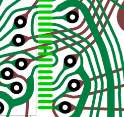
In printed circuit boards, teardrops are typically drop-shaped features at the junction of vias (teardrop vias) or contact pads (teardrop pads) and traces (teardrop traces).
Purpose
The main purpose of teardrops is to enhance structural integrity in presence of thermal or mechanical stresses,[1][2][3] for example due to vibration or flexing.[4] Structural integrity may be compromised, e.g., by misalignment during drilling, so that too much copper may be removed by the drill hole in the area where a trace connects to the pad or via.[2][3][5] An extra advantage is the enlarging of manufacturing tolerances, making manufacturing easier and cheaper.[3]
While a typical shape of a teardrop is straight-line tapering, they may be concave.[2] This type of teardrop is also called filleting or straight.[3] To produce a snowman-shaped teardrop, a secondary pad of smaller size is added at the junction overlapping with the primary pad (hence the nickname).[3][6]
Necking
For similar reasons, a technique called trace necking reduces (or necks down[7][8][9]) the width of a trace that approaches a narrower pad of a surface-mounted device or a through-hole with a diameter that is less than the width of the trace, or when the trace passes through bottlenecks (for example, between the pads of a component).[8][9][10][11]
References
- ↑ "Component placement tips and strategies". EDN Network. 2014-02-21. http://www.edn.com/design/pc-board/4428665/2/Component-placement-tips-and-strategies.
- ↑ 2.0 2.1 2.2 "Removing Unused Pads and Adding Teardrops". Altium Designer technical documentation. Altium. 2017-05-30. http://www.altium.com/documentation/17.1/display/ADES/((Removing+Unused+Pads+and+Adding+Teardrops))_AD.
- ↑ 3.0 3.1 3.2 3.3 3.4 "Why Where When and how teardrops should be added to PCB?". KaiZen Technologies. 2010. http://www.kaizen-t.com/technical/teardropinpcb.html.
- ↑ Ruth (2023-04-28). "Introduction to high speed PCB and is it same as high frequency PCB ?" (in en-US). https://www.pcbaaa.com/an-ultimate-introduction-to-high-speed-pcb-and-is-it-same-as-high-frequency-pcb/.
- ↑ "Empfehlung zu Tear-drops" (in German). AT&S AG, Fachverband Elektronik-Design e.V. (FEV). October 2002. http://wiki.fed.de/images/5/50/Empfehlung_zu_Tear-drops.pdf.
- ↑ "PCB Design Guidelines for 0.5mm Package-on-Package Applications Processor, Part I". Texas Instruments. June 2010. http://www.ti.com/lit/an/sprabb3/sprabb3.pdf.
- ↑ "Interactive Routing". Altium Designer technical documentation. Altium. 2017-04-25. http://www.altium.com/documentation/17.1/display/ADES/((Interactive+Routing))_AD.
- ↑ 8.0 8.1 Printed Circuit Board Design with Microcomputers (1 ed.). New York, USA: Intertext Publications/Multiscience Press, Inc., McGraw-Hill Book Company. 1991-08-01. p. 102. ISBN 0-07-009558-2. https://dl.acm.org/citation.cfm?id=114661.
- ↑ 9.0 9.1 "11.1.3 Packaging Electronic Systems - Design of Printed Wiring Boards". The Electronics Handbook (2 ed.). CRC Press, Taylor & Francis Group, LLC. 2005. p. 1266. ISBN 978-0-8493-1889-4. http://s1.downloadmienphi.net/file/downloadfile6/192/1385077.pdf. Retrieved 2017-09-25.
- ↑ Abrams, Halle, "Packaging Electronic Systems", US patent 3560256, published 1971-02-02
- ↑ [1.House.High.speed.Circuit.Board.Signal.Integrity.eBook.pdf High-Speed Circuit Board Signal Integrity] (1 ed.). Norwood, MA, USA: Artech House, Inc.. 2004. pp. 104–105. ISBN 1-58053-131-8. http://plrtzglrb.hu/ghz/books/Artech[1].House.High.speed.Circuit.Board.Signal.Integrity.eBook.pdf. Retrieved 2017-09-26.
External links
- PCB Prototype Manufacturing
 |  |
Categories: [Printed circuit board manufacturing]
↧ Download as ZWI file | Last modified: 03/11/2024 22:23:43 | 3 views
☰ Source: https://handwiki.org/wiki/Engineering:Teardrop_(electronics) | License: CC BY-SA 3.0