Hardware Register
 From Handwiki
In digital electronics, a register is a group of memory cells that store a collection of bits and continuously output the stored data.[1][2] It typically consists of a synchronized group of flip-flops in which each flip-flop stores and outputs one bit of the collection.[3][4][5] The number of bits a register can store, known as its word size, is equal to the number of flip-flops it contains.[6][1] It is volatile memory, meaning that the circuit will cease to retain its stored data upon loss of operating power.[6] Registers are characterized in various ways, including by bit storage capacity (e.g., 32-bit register), signal polarities, logic level and power supply voltages, and timing parameters.[3]
Registers are a fundamental building block of digital systems. They are used in a diverse range of applications, including in central processing units (CPUs) for a variety of purposes; in digital counters and other state machines; in serial and parallel communication; and in device interfaces for functions such as control and configuration, status reporting, and data buffering.
Signals
A register has a variety of input and output nets, which are the electrical conductors used to convey digital signals between the register and external circuitry.
A register has inputs that receive the data to be stored, and outputs that emit the currently stored data.[6][3] Its flip-flops share a common clock input which, upon relevant signal edges, causes the flip-flops to sample and store the input data.[3][5][7] Typically, the flip-flops also share a common reset input, which is used to initialize the stored data.[4]
Input signals
- Reset — initializes all flip-flops to known states, typically 0. Depending on the register design, this may be synchronous or asynchronous.[3] This is typically used to zero the flip-flops before starting clocked operation.[4]
- Clock — upon rising or falling signal edge (the active edge[3]), causes the data presented on the data inputs to be stored in the register's flip-flops. In registers that have a synchronous reset input in which reset is asserted, a clock active edge will invoke a register reset in lieu of storing input data.
- Data in — data to be stored upon clock active edge, one bit per flip-flop. For a register with flip-flops, the data inputs are typically named to .
Output signals
- Data out — currently stored data, one bit per flip-flop, continuously emitted, stable except when transitioning to new stored values. For a register with flip-flops, these are typically designated to . Some registers provide both true and complementary data outputs. For example, the 74175 MSI integrated circuit has four flip flops, each with its true and complementary outputs bonded out to package pins.
Unused signals
Unused inputs are usually connected to fixed logic levels to prevent them from floating, which might cause unpredictable behavior or damage the register's circuitry.
Unused outputs are typically left unconnected.
Data structure
The data stored in a register may represent any arbitrary binary data that fits into the register's storage capacity. In cases where the data represents a binary integer, the least to most significant data bits are typically associated with register inputs to and outputs to respectively, although this is not required.
Implementation
Registers are implemented in various ways, including as stand-alone MSI integrated circuits, as integrated registers within ASICs and programmable processors, and as IP blocks in FPGAs. In the latter case, a register is typically instantiated by synthesizing it from a description written in VHDL, Verilog or some other hardware description language. For example, the following VHDL code describes a 32-bit register with load enable and asynchronous reset:
entity reg32 is -- 32 bit register with load enable
  port (
    CLK   : in  std_logic;                     -- clock
    RESET : in  std_logic;                     -- async reset
    LD    : in  std_logic;                     -- load enable
    D     : in  std_logic_vector(31 downto 0); -- data inputs
    Q     : out std_logic_vector(31 downto 0)  -- stored data
  );
end reg32;

architecture behavioral of reg32 is
begin
  process(CLK, RESET)
  begin
    if RESET = '1' then          -- if RESET asserted
      Q <= (others => '0');      --   zero stored data
    elsif rising_edge(CLK) then  -- else if CLK active edge
      if LD = '1' then           --   and loading is allowed
        Q <= D;                  --     store input data
      end if;
    end if;                      -- else retain stored data
  end process;
end behavioral;
In stand-alone MSI integrated circuits, a register is implemented as a semiconductor die which is bonded and encapsulated in a semiconductor package.[8]
-
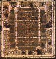 Semiconductor die of an 8-bit register (Motorola MC74HCT374A)
 -
 Assembled 8-bit register in a plastic dual-in-line package (Texas Instruments SN74S374N)


Signal visibility
Depending on its implementation and purpose, a register's data inputs and outputs may all be public (accessible to external circuitry), or some data inputs or outputs (or both) may be designated for internal use only. An example of the latter is a serial-in serial-out shift register, which exposes only one data input and one data output to external circuitry.
Applications
In many applications, combinational logic is used to control when and how new data is stored in a register.[1] For example, registers are commonly endowed with a Template:Dfni function that employs logic gates, in conjunction with a Template:Dfni signal, to allow or inhibit new data to be stored.[3] In a parallel-input shift register, logic gates are used to transfer each stored bit to an adjacent flip-flop, thus shifting the stored binary word by one bit position in a single clock cycle.[3] In a synchronous binary counter, logic gates cause the stored value to step through a binary count sequence.
In bus-organized systems, multiplexers or tri-state buffers (or both) are used to route register outputs onto shared buses.[3] Common examples of this include register files, peripheral interfaces and multiplexed address/data buses. To facilitate this, address decoders are often used to select one from among a group of registers to input data from, or send stored data to, a shared bus. For example, in computers, peripheral interface registers are often accessed in a fashion similar to random access memory (RAM), by using a memory or port address to select a particular register.[9]
Load enable
In many applications, it is required to load (store new data in) a register only during specific clock cycles and to hold (retain currently stored data) during other clock cycles. This is facilitated by adding a load enable function to the register, which consists of logic gates and an associated control input — typically called Template:Dfni (CE), Template:Dfni or simply Template:Dfni (LD) — that allows or inhibits loading depending on its state.
A simple way to implement this is to gate the register's clock input with the control signal, but this interferes with system timing because it introduces propagation delay into the clock's signal path.[4] Instead, to avoid problematic clock skew, the control signal typically is used to manage signal routing to the register's data inputs[4] via primitives such as those shown below.
-
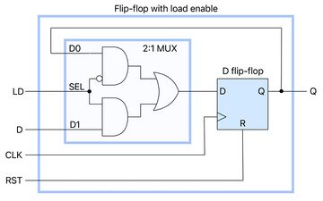 In this primitive, load enable (LD) controls a 2-to-1 multiplexer which routes either the data input (D) or the current state (Q) to the flip-flop's D input, thus causing the memory cell to load or hold, respectively
 -
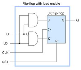 In this primitive, a JK flip-flop uses two gates to implement load enable. When LD is asserted, the flip-flop is set or cleared depending on D, thus effectively storing D. When LD is negated, the stored data remains unchanged.
 -
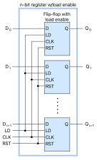 An n-bit register with load enable, constructed from n primitives


Addressable registers
In bus-oriented systems, it is common for registers to receive data from or send stored data to (or both) a shared bus. Widely used examples of this include register files and peripheral interface registers. To facilitate this, each register is assigned a unique binary number known as its address, which is used to select the register for read and write operations. The selection mechanism is often based on a 1-of-n binary decoder, which in this capacity is commonly referred to as an address decoder. A register that can be accessed and manipulated using a specific address is said to be an addressable register.[1]
To simplify access and management, related registers are typically organized into groups in which each group is assigned a contiguous range of addresses.[10] In general, it is not required for every address in the range to be assigned to a register, and a register may be assigned multiple addresses in the range.
The registers in a group typically share a data input bus for write operations, or a data output bus for read operations, or both. In the latter case, depending on the application, a register group may use separate buses for read and write operations or a single bus for both.
Write operation
In a write operation, an addressable register is selected by sending its address to an address decoder (typically a binary decoder). When enabled, the address decoder will in turn enable the selected register to store new data. The register's data inputs are connected to and thus receive the data to be stored from a shared bus. Upon active edge at its clock input, the selected register will store the word presented on the data bus.
Depending on the data bus architecture, the register's clock signal may consist of write strobes (one pulse per write) or it may be a continuous clock (stream of periodic pulses). The latter is characteristic of systems that employ synchronous parallel buses (e.g., FPGAs, ASICSs, processor register files) in which it is standard practice to synchronize all storage elements with a continuous clock,[6][11] whereas pulse-per-write clocking is characteristic of asynchronous parallel buses (e.g., peripheral I/O registers).[6] Example circuits of both are shown below.
-
 Synchronous parallel bus example.
Write enable (WE) is asserted and the register address (ADDR) is sent to the binary decoder, causing it to assert the selected register's clock enable input (CE). Upon clock (CLK) rising edge, the register will store the word presented on the data bus (DATA). WE is typically generated by a finite-state machine. -
 Asynchronous parallel bus example.
Enable (EN) is asserted and the register address (ADDR) is sent to the binary decoder, causing it to assert the selected register's clock enable input (CE). Upon write (WR) rising edge (the trailing edge of active-low WR strobe, in this example), the selected register will store the word presented on the data bus (DATA). EN is often generated by a separate address decoder that qualifies higher-order address bits (e.g., chip select).


Read operation
The process of reading an addressable register involves gating its output data onto a shared bus. Depending on the application, the gating mechanism may employ multiplexers or tri-state buffers, or both. The outputs of all registers in a group are accessible to the gating mechanism, thus allowing any register's output word to be sent to the bus. Some applications employ multiple instances of this mechanism to allow different registers (or a single register) to be concurrently gated onto multiple buses; each such instance is commonly called a read port.[6]
- Multiplexer gating
In multiplexer-based gating, a register is selected for a read operation by sending its address to a multiplexer. The multiplexer then routes the register's output word to the bus either directly, as shown below, or through a tri-state word buffer in cases where the bus may be driven by other signal sources.
-
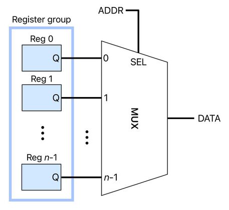 During a register read operation, the target register's address (ADDR) is sent to the word multiplexer, which responds by driving the register's stored data onto the shared bus (DATA).

- Tri-state buffer gating
In tri-state buffer-based gating, a register is selected for a read operation by sending its address to a binary decoder, causing the decoder to assert its associated output signal. This signal is sent to a tri-state word buffer, which responds by gating the register's output data onto the bus.
-
 During a register read operation, output enable (OE) is asserted and the target register's address (ADDR) is sent to a binary decoder. This causes the decoder to enable the associated tri-state word buffer, which in turn gates the register's stored data onto a shared bus (DATA).

Atomic bit operations
In multitasking systems it is often necessary to set or clear select register bits while leaving others unchanged. This can be accomplished purely by software via a read–modify–write (RMW) sequence, but if the register is accessed by multiple processes or cores, the integrity of each RMW must be protected using mechanisms such as memory barriers, atomic instructions, and semaphores. The required protection is further complicated if the register can be modified by direct memory access (DMA) transfers.
RMWs and their protection mechanisms can be avoided if the register directly supports atomic operations. Registers endowed with this capability inherently allow specified bits to be set or cleared without the risk of interference from DMA or other processes. This is typically implemented by adding logic to the input of each flip-flop such as in the example below:
-
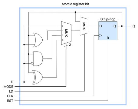 In this circuit primitive, MODE is a two-bit binary value that selects the operation to be performed. In mode 0, D is unconditionally stored. In modes 1 to 3, Q is modified (set, cleared or complemented, respectively) when D is '1', or unchanged when D is '0'. LD is a master enable that allows or inhibits changes to Q.
 -
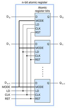 n-bit atomic register with load enable, constructed from n primitives


In the above circuits, any arbitrary combination of bits can be atomically modified. For example, in the case of a 16-bit register, to atomically set bits 8 and 10, external circuitry would assert LD='1', MODE='1' and D[15:0]=0x0500.
The MODE inputs may be driven by low order bits of an address bus, thus mapping each of the register's four operations to a unique address. Alternatively, MODE may driven by otherwise unused data bus bits, which allows the register to be mapped to a single address.
Shift registers
A shift register is a register which is capable of shifting its stored word by one bit position in a single clock cycle.[1][12] The shift is accomplished by simultaneously writing the bit stored in each memory cell to its neighboring cell.
Depending on the shift register design, the memory cells are either physically or logically connected together (via multiplexers or other combinational logic) in a "chain" such that the output of each cell is applied to the input of an adjacent cell.[1] When executing a shift operation, the data input of the first cell acts as serial data input to the chain and the output of the last cell serves as serial data output.[1]
A shift register may have serial or parallel (or both) data inputs, and serial or parallel (or both) data outputs.[12] A clock enable input is often available to qualify clock edges and thereby allow or inhibit changes to the stored data. Shift registers with parallel inputs usually have a load/shift input which determines whether the register, upon next qualified clock edge, will store the parallel input data or perform a shift operation.
Shift registers are used in a variety of ways. Common uses include serial-to-parallel and parallel-to-serial conversion in communication systems,[12] metastability avoidance when crossing clock domains, and as ring or Johnson counters to generate one-hot or Gray code sequences in finite state machines.
Serial-in serial-out shift register Serial-in parallel-out shift register Parallel-in serial-out shift register
Interrupt status register
Some register bits are not set or cleared purely as a function of a single data source. An example of this is the circuit shown below, which uses a JK flip-flop to store the status of an interrupt request. The flip-flop is set by a device service request and cleared when the request is acknowledged.[13] The register output is sent to an interrupt controller to request a processor interrupt.[13]
-
 Example interrupt status register bit, used to generate an interrupt request (IRQ). The flip-flop is set by a device service request and cleared upon request acknowledge.
 -
 Typical application: addressable interrupt status register. Register access is enabled via SEL, which is typically driven by an address decoder that maps the register into a processor's memory or I/O address space. The processor can read the register to determine the IRQ state. When the request is no longer needed, the processor signals ACK by writing 1 to the register (writing 0 has no effect), thus invoking an atomic clear.


Computers
In computers, typical uses of registers include:
- The registers in a central processing unit (CPU), which are called processor registers
- configuration and start-up of certain features, especially during initialization
- buffer storage e.g. video memory for graphics cards
- input/output (I/O) of different kinds
- determining the source of an interrupt
- peripheral status reporting such as whether a certain event has occurred, for example, a modem status register or a line status register
Peripherals
Registers are used in interfaces between software and peripherals. Software writes them to send information to the device, and reads them to receive information from the device.
To read or write a register in a Template:Dfni (computer hardware outside the CPU), the processor executes a load or store instruction using the register's memory-mapped I/O or port-mapped I/O address. Registers are accessed in words, but sometimes only use a few bits of the word.
From a CPUs perspective, a register is either read/write, read-only or write-only. The latter is generally not preferred as it can make debugging difficult and prevent read–modify–write operations.
The software-accessible registers in standard integrated circuits are typically documented in their associated electronic component datasheets. Many such devices also have internal registers that are inaccessible to software, which are used for purposes such as state machines and pipelining.
Various standards exist that can be used to specify and describe addressable and other registers via XML, such as IP-XACT and Common Microcontroller Software Interface Standard (CMSIS).
See also
- Register-transfer level (RTL)
References
- ↑ 1.0 1.1 1.2 1.3 1.4 1.5 1.6 Mano , Morris ; Ciletti , Michael (2017 ). Digital Design With an Introduction to the Verilog HDL, VHDL, and SystemVerilog . Pearson . ISBN 978-0134549897.
- ↑ Maini , Anil (2007 ). Digital Electronics . Wiley . ISBN 978-0470032145.
- ↑ 3.0 3.1 3.2 3.3 3.4 3.5 3.6 3.7 3.8 Brown , Stephen ; Vranesic , Zvonko (2009 ). Fundamentals of Digital Logic with VHDL Design . McGraw Hill . ISBN 978-0073529530.
- ↑ 4.0 4.1 4.2 4.3 4.4 Mano , M. Morris . Digital Logic and Computer Design . Pearson . ISBN 978-0132145107.
- ↑ 5.0 5.1 Tanenbaum , Andrew ; Austin , Todd (2013 ). Structured Computer Organization . Pearson . ISBN 978-0132916523.
- ↑ 6.0 6.1 6.2 6.3 6.4 6.5 Patterson , David ; Hennessy , John . Computer Organization and Design: The Hardware/Software Interface . Morgan Kaufmann . ISBN 978-0123747501.
- ↑ Roth , Charles ; Kinney , Larry . Fundamentals of Logic Design . Cengage . ISBN 978-1337620352.
- ↑ Brock, Les (1970) (in en). Designing With MSI. Signetics.
- ↑ Rajaraman, V.; Radhakrishnan, T. (2007-06-01) (in en). Computer Organization and Architecture. PHI Learning Pvt. Ltd.. pp. 38. ISBN 978-8120332003. https://books.google.com/books?id=hZQ4jAdpUAAC&pg=SA3-PA37.
- ↑ Kamal , Raj . Microcontrollers: Architecture, Programming, Interfacing and System Design . Pearson . ISBN 978-8131706978.
- ↑ Brown, Stephen; Vranesic, Zvonko. Fundamentals of Digital Logic with VHDL Design. McGraw Hill. ISBN 978-0-07-338054-4.
- ↑ 12.0 12.1 12.2 Balch, Mike. Complete Digital Design / A Comprehensive Guide to Digital Electronics and Computer System Architecture. McGraw-Hill Inc.. ISBN 0-07-143347-3.
- ↑ 13.0 13.1 Stringham , Gary . Hardware/Firmware Interface Design: Best Practices for Improving Embedded Systems Development . Newnes . ISBN 978-1856176057.
pt:Registro
 |  |
Categories: [Control flow] [Central processing unit] [Digital registers]
↧ Download as ZWI file | Last modified: 08/21/2026 12:16:18 | 8 views
☰ Source: https://handwiki.org/wiki/Hardware_register | License: CC BY-SA 3.0
 KSF
KSF