List Of Intel Microprocessors
 From Handwiki
This generational list of Intel processors attempts to present all of Intel's processors from the pioneering 4-bit 4004 (1971) to the present high-end offerings. Concise technical data is given for each product.
Latest
10th generation Core/Comet Lake/Ice Lake
| Model | Price (USD) | Cores | Threads | Clock rate (GHz) | Cache (MB) | IGP | TDP (W) | Codename | Socket | Release | |||||
|---|---|---|---|---|---|---|---|---|---|---|---|---|---|---|---|
| base | max turbo | L1 | L2 | L3 | processor | Clock rate (MHz) | |||||||||
| base | max dynamic | ||||||||||||||
| i7-1065G7 | $426 | 4 | 8 | 1.30 | 3.90 | N/A | N/A | 8 | Iris Plus | 300 | 1100 | 15 | Ice Lake | BGA 1526 | Q3 2019 |
| i7-1060G7 | 4 | 8 | 1.00 | 3.80 | N/A | N/A | 8 | Iris Plus | 300 | 1100 | 9 | Ice Lake | Q3 2019 | ||
| i7-10710U | $443 | 6 | 12 | 1.10 | 4.70 | N/A | N/A | 12 | UHD | 300 | 1150 | 15 | Comet Lake | BGA 1528 | Q3 2019 |
| i7-10510U | $409 | 4 | 8 | 1.80 | 4.90 | N/A | N/A | 8 | UHD | 300 | 1150 | 15 | Comet Lake | BGA 1528 | Q3 2019 |
| i7-10510Y | $403 | 4 | 8 | 1.20 | 4.50 | N/A | N/A | 8 | UHD | 300 | 1150 | 7 | Amber Lake Y | UTFCBGA1377 | Q3 2019 |
9th generation Core/Coffee Lake Refreshed
| Model | Price (USD) | Cores | Threads | Clock rate (GHz) | Cache (MB) | IGP | TDP (W) | Codename | Socket | Release | |||||
|---|---|---|---|---|---|---|---|---|---|---|---|---|---|---|---|
| base | max turbo | L1 | L2 | L3 | processor | Clock rate (MHz) | |||||||||
| base | max dynamic | ||||||||||||||
| i9-9900K | $499 | 8 | 16 | 3.60 | 5.00 | N/A | N/A | 16 | UHD 630 | 350 | 1200 | 95 | Coffee Lake | LGA 1151 | Q4 2018 |
| i7-9700K | $385 | 8 | 8 | 3.60 | 4.90 | N/A | N/A | 12 | UHD 630 | 350 | 1200 | 95 | Coffee Lake | LGA 1151 | Q4 2018 |
| i5-9600K | $263 | 6 | 6 | 3.70 | 4.60 | N/A | N/A | 9 | UHD 630 | 350 | 1150 | 95 | Coffee Lake | LGA 1151 | Q4 2018 |
| i5-9400F | $149 | 6 | 6 | 2.90 | 4.10 | N/A | N/A | 9 | N/A | N/A | N/A | 65 | Coffee Lake | LGA 1151 | Q1 2019 |
| i3-9350KF | $159 | 4 | 4 | 4.00 | 4.60 | N/A | N/A | 8 | N/A | N/A | N/A | 91 | Coffee Lake | LGA 1151 | Q1 2019 |
8th generation Core/Coffee Lake/Kaby Lake Refresh/Whiskey Lake
Desktop
| Model | Price (USD) | Cores | Threads | Clock rate (GHz) | Cache (MB) | IGP | TDP (W) | Codename | Socket | Release | |||||
|---|---|---|---|---|---|---|---|---|---|---|---|---|---|---|---|
| base | max turbo | L1 | L2 | L3 | processor | Clock rate (MHz) | |||||||||
| base | max dynamic | ||||||||||||||
| i7-8700K | $359 | 6 | 12 | 3.70 | 4.70 | N/A | N/A | 12 | UHD 630 | 350 | 1200 | 95 | Coffee Lake | LGA 1151 | Q4 2017 |
| i7-8700 | $303 | 6 | 12 | 3.20 | 4.60 | N/A | N/A | 12 | UHD 630 | 350 | 1200 | 65 | Coffee Lake | LGA 1151 | Q4 2017 |
| i7-8086K | $425 | 6 | 12 | 4.00 | 5.00 | N/A | N/A | 12 | UHD 630 | 350 | 1200 | 95 | Coffee Lake | LGA 1151 | Q2 2018 |
| i5-8600K | $257 | 6 | 6 | 3.60 | 4.30 | N/A | N/A | 9 | UHD 630 | 350 | 1150 | 95 | Coffee Lake | LGA 1151 | Q4 2017 |
| i5-8500 | $202 | 6 | 6 | 3.00 | 4.10 | N/A | N/A | 9 | UHD 630 | 350 | 1100 | 65 | Coffee Lake | LGA 1151 | Q2 2018 |
| i5-8400 | $182 | 6 | 6 | 2.80 | 4.00 | N/A | N/A | 9 | UHD 630 | 350 | 1050 | 65 | Coffee Lake | LGA 1151 | Q4 2017 |
| i3-8350K | $168 | 4 | 4 | 4.00 | N/A | N/A | N/A | 8 | UHD 630 | 350 | 1150 | 91 | Coffee Lake | LGA 1151 | Q4 2017 |
| i3-8100 | $117 | 4 | 4 | 3.60 | N/A | N/A | N/A | 6 | UHD 630 | 350 | 1100 | 65 | Coffee Lake | LGA 1151 | Q4 2017 |
Mobile
| Model | Price (USD) | Cores | Threads | Clock rate (GHz) | Cache (MB) | IGP | TDP (W) | Codename | Socket | Release | |||||
|---|---|---|---|---|---|---|---|---|---|---|---|---|---|---|---|
| base | max turbo | L1 | L2 | L3 | processor | Clock rate (MHz) | |||||||||
| base | max dynamic | ||||||||||||||
| m3-8100Y | $281 | 2 | 4 | 1.10 | 3.40 | 0.125 | 0.5 | 4 | UHD 615 | 300 | 900 | 5 | Amber Lake Y | BGA 1515 | Q3 2018 |
| i9-8950HK | $583 | 6 | 12 | 2.90 | 4.80 | 0.375 | 1.5 | 12 | UHD 630 | 350 | 1200 | 45 | Coffee Lake | BGA 1440 | Q2 2018 |
| i7-8850H | $395 | 6 | 12 | 2.60 | 4.30 | 0.375 | 1.5 | 9 | UHD 630 | 350 | 1150 | 45 | Coffee Lake | BGA 1440 | Q2 2018 |
| i7-8750H | $395 | 6 | 12 | 2.20 | 4.10 | 0.375 | 1.5 | 9 | UHD 630 | 350 | 1100 | 45 | Coffee Lake | BGA 1440 | Q2 2018 |
| i7-8700B | $303 | 6 | 12 | 3.20 | 4.60 | 0.375 | 1.5 | 12 | UHD 630 | 350 | 1200 | 65 | Coffee Lake | BGA 1440 | Q2 2018 |
| i7-8665U | $409 | 4 | 8 | 1.90 | 4.80 | 0.25 | 1 | 8 | UHD 620 | 300 | 1150 | 15 | Whiskey Lake | BGA 1528 | Q2 2019 |
| i7-8650U | $409 | 4 | 8 | 1.90 | 4.20 | 0.25 | 1 | 8 | UHD 620 | 300 | 1150 | 15 | Kaby Lake R | BGA 1356 | Q3 2017 |
| i7-8569U | $431 | 4 | 8 | 2.80 | 4.70 | N/A | N/A | 8 | Iris Plus 655 | 300 | 1200 | 28 | Coffee Lake | BGA 1528 | Q2 2019 |
| i7-8565U | $409 | 4 | 8 | 1.80 | 4.60 | 0.25 | 1 | 8 | UHD | 300 | 1150 | 15 | Whiskey Lake | BGA 1528 | Q3 2018 |
| i7-8559U | $431 | 4 | 8 | 2.70 | 4.50 | 0.25 | 1 | 8 | Iris Plus 655 | 300 | 1200 | 28 | Coffee Lake | BGA 1528 | Q2 2018 |
| i7-8557U | $431 | 4 | 8 | 1.70 | 4.50 | 0.25 | 1 | 8 | Iris Plus 645 | 300 | 1150 | 15 | Coffee Lake | BGA 1528 | Q3 2019 |
| i7-8550U | $409 | 4 | 8 | 1.80 | 4.00 | 0.25 | 1 | 8 | UHD 620 | 300 | 1150 | 15 | Kaby Lake R | BGA 1356 | Q3 2017 |
| i7-8500Y | $393 | 2 | 4 | 1.50 | 4.20 | 0.125 | 0.5 | 4 | UHD 615 | 300 | 1050 | 5 | Amber Lake Y | BGA 1515 | Q1 2019 |
| i5-8500B | $192 | 6 | 6 | 3.00 | 4.10 | 0.375 | 1.5 | 9 | UHD 630 | 350 | 1100 | 65 | Coffee Lake | BGA 1440 | Q2 2018 |
| i5-8400H | $250 | 4 | 8 | 2.50 | 4.20 | 0.25 | 1 | 8 | UHD 630 | 350 | 1100 | 45 | Coffee Lake | BGA 1440 | Q2 2018 |
| i5-8400B | $182 | 6 | 6 | 2.80 | 4.00 | 0.375 | 1.5 | 9 | UHD 630 | 350 | 1050 | 65 | Coffee Lake | BGA 1440 | Q2 2018 |
| i5-8365U | $297 | 4 | 8 | 1.60 | 4.10 | 0.25 | 1 | 6 | UHD | 300 | 1100 | 15 | Whiskey Lake | BGA 1528 | Q2 2019 |
| i5-8350U | $297 | 4 | 8 | 1.70 | 3.60 | 0.25 | 1 | 6 | UHD 620 | 300 | 1100 | 15 | Kaby Lake R | BGA 1356 | Q3 2017 |
| i5-8310Y | $281 | 2 | 4 | 1.60 | 3.90 | 0.125 | 0.5 | 4 | UHD 617 | 300 | 1050 | 7 | Amber Lake Y | BGA 1515 | Q1 2019 |
| i5-8300H | $250 | 4 | 8 | 2.30 | 4.00 | 0.25 | 1 | 8 | UHD 630 | 350 | 1000 | 45 | Coffee Lake | BGA 1440 | Q2 2018 |
| i5-8269U | $320 | 4 | 8 | 2.60 | 4.20 | 0.25 | 1 | 6 | Iris Plus 655 | 300 | 1100 | 28 | Coffee Lake | BGA 1528 | Q2 2018 |
| i5-8265U | $297 | 4 | 8 | 1.60 | 3.90 | 0.25 | 1 | 6 | UHD | 300 | 1100 | 15 | Whiskey Lake | BGA 1528 | Q3 2018 |
| i5-8260U | $297 | 4 | 8 | 1.60 | 3.90 | N/A | N/A | 6 | UHD 620 | 300 | 1100 | 15 | Coffee Lake | BGA 1528 | Q4 2019 |
| i5-8259U | $320 | 4 | 8 | 2.30 | 3.80 | 0.25 | 1 | 6 | Iris Plus 655 | 300 | 1050 | 28 | Coffee Lake | BGA 1528 | Q2 2018 |
| i5-8257U | $320 | 4 | 8 | 1.40 | 3.90 | 0.25 | 1 | 6 | Iris Plus 645 | 300 | 1050 | 15 | Coffee Lake | BGA 1528 | Q3 2019 |
| i5-8250U | $297 | 4 | 8 | 1.60 | 3.40 | 0.25 | 1 | 6 | UHD 620 | 300 | 1100 | 15 | Kaby Lake R | BGA 1356 | Q3 2017 |
| i5-8210Y | $281 | 2 | 4 | 1.60 | 3.60 | 0.125 | 0.5 | 4 | UHD 617 | 300 | 1050 | 7 | Amber Lake Y | BGA 1515 | Q1 2019 |
| i5-8200Y | $291 | 2 | 4 | 1.30 | 3.90 | 0.125 | 0.5 | 4 | UHD 615 | 300 | 950 | 5 | Amber Lake Y | BGA 1515 | Q3 2018 |
| i3-8145U | $281 | 2 | 4 | 2.10 | 3.90 | 0.125 | 0.5 | 4 | UHD | 300 | 1000 | 15 | Whiskey Lake | BGA 1528 | Q3 2018 |
| i3-8140U | $281 | 2 | 4 | 2.10 | 3.90 | N/A | N/A | 4 | UHD 620 | 300 | 1000 | 15 | Coffee Lake | BGA 1528 | Q4 2019 |
| i3-8130U | $281 | 2 | 4 | 2.20 | 3.40 | 0.125 | 0.5 | 4 | UHD 620 | 300 | 1000 | 15 | Kaby Lake R | BGA 1356 | Q1 2018 |
| i3-8109U | $304 | 2 | 4 | 3.00 | 3.60 | 0.125 | 0.5 | 4 | Iris Plus 655 | 300 | 1050 | 28 | Coffee Lake | BGA 1528 | Q2 2018 |
| i3-8100H | $225 | 4 | 4 | 3.00 | N/A | 0.25 | 1 | 6 | UHD 630 | 350 | 1000 | 45 | Coffee Lake | BGA 1440 | Q3 2018 |
| i3-8100B | $133 | 4 | 4 | 3.60 | N/A | N/A | N/A | 6 | UHD 630 | 350 | 1050 | 65 | Coffee Lake | BGA 1440 | Q3 2018 |
7th generation Core/Kaby Lake/Skylake (X-series Processors)/Apollo Lake
Desktop version
| Model | Price (USD) | Cores | Threads | Clock rate (GHz) | Cache (MB) | IGP | TDP (W) | Codename | Socket | Release | |||||
|---|---|---|---|---|---|---|---|---|---|---|---|---|---|---|---|
| base | max turbo | L1 | L2 | L3 | processor | Clock rate (MHz) | |||||||||
| base | max dynamic | ||||||||||||||
| i9-7980XE | $1999 | 18 | 36 | 2.60 | 4.20 | N/A | N/A | 24.75 | N/A | N/A | N/A | 165 | Skylake | LGA 2066 | Q3 2017[1] |
| i9-7960X | $1699 | 16 | 32 | 2.80 | 4.20 | N/A | N/A | 22.00 | N/A | N/A | N/A | 165 | Skylake | LGA 2066 | Q3 2017[1] |
| i9-7940X | $1399 | 14 | 28 | 3.10 | 4.30 | N/A | N/A | 19.25 | N/A | N/A | N/A | 165 | Skylake | LGA 2066 | Q3 2017[1] |
| i9-7920X | $1189 | 12 | 24 | 2.90 | 4.30 | N/A | N/A | 16.50 | N/A | N/A | N/A | 140 | Skylake | LGA 2066 | Q3 2017 |
| i9-7900X | $989 | 10 | 20 | 3.30 | 4.30 | N/A | N/A | 13.75 | N/A | N/A | N/A | 140 | Skylake | LGA 2066 | Q2 2017 |
| i7-7820X | $589 | 8 | 16 | 3.60 | 4.30 | N/A | N/A | 11.00 | N/A | N/A | N/A | 140 | Skylake | LGA 2066 | Q2 2017 |
| i7-7800X | $383 | 6 | 12 | 3.50 | 4.00 | N/A | N/A | 8.25 | N/A | N/A | N/A | 140 | Skylake | LGA 2066 | Q2 2017 |
| i7-7740X | $339 | 4 | 8 | 4.30 | 4.50 | N/A | N/A | 8 | N/A | N/A | N/A | 112 | Kaby Lake | LGA 2066 | Q1 2017 |
| i7-7700K | $350 | 4 | 8 | 4.20 | 4.50 | N/A | N/A | 8 | HD 630 | 350 | 1150 | 91 | Kaby Lake | LGA 1151 | Q1 2017 |
| i7-7700 | $303 | 4 | 8 | 3.60 | 4.20 | N/A | N/A | 8 | HD 630 | 350 | 1150 | 65 | Kaby Lake | LGA 1151 | Q1 2017 |
| i7-7700T | $303 | 4 | 8 | 2.90 | 3.80 | N/A | N/A | 8 | HD 630 | 350 | 1150 | 35 | Kaby Lake | LGA 1151 | Q1 2017 |
| i5-7640X | $242 | 4 | 4 | 4.00 | 4.20 | N/A | N/A | 6 | N/A | N/A | N/A | 112 | Kaby Lake | LGA 2066 | Q1 2017 |
| i5-7600K | $243 | 4 | 4 | 3.80 | 4.20 | N/A | N/A | 6 | HD 630 | 350 | 1150 | 91 | Kaby Lake | LGA 1151 | Q1 2017 |
| i5-7600 | $224 | 4 | 4 | 3.50 | 4.10 | N/A | N/A | 6 | HD 630 | 350 | 1150 | 65 | Kaby Lake | LGA 1151 | Q1 2017 |
| i5-7600T | $224 | 4 | 4 | 2.80 | 3.70 | N/A | N/A | 6 | HD 630 | 350 | 1100 | 35 | Kaby Lake | LGA 1151 | Q1 2017 |
| i5-7500 | $192 | 4 | 4 | 3.40 | 3.80 | N/A | N/A | 6 | HD 630 | 350 | 1100 | 65 | Kaby Lake | LGA 1151 | Q1 2017 |
| i5-7500T | $192 | 4 | 4 | 2.70 | 3.30 | N/A | N/A | 6 | HD 630 | 350 | 1100 | 35 | Kaby Lake | LGA 1151 | Q1 2017 |
| i5-7400 | $182 | 4 | 4 | 3.00 | 3.50 | N/A | N/A | 6 | HD 630 | 350 | 1000 | 65 | Kaby Lake | LGA 1151 | Q1 2017 |
| i5-7400T | $187 | 4 | 4 | 2.40 | 3.00 | N/A | N/A | 6 | HD 630 | 350 | 1000 | 35 | Kaby Lake | LGA 1151 | Q1 2017 |
| i3-7350K | $179 | 2 | 4 | 4.20 | N/A | N/A | N/A | 4 | HD 630 | 350 | 1150 | 60 | Kaby Lake | LGA 1151 | Q1 2017 |
| i3-7320 | $157 | 2 | 4 | 4.10 | N/A | N/A | N/A | 4 | HD 630 | 350 | 1150 | 51 | Kaby Lake | LGA 1151 | Q1 2017 |
| i3-7300 | $147 | 2 | 4 | 4.00 | N/A | N/A | N/A | 4 | HD 630 | 350 | 1150 | 51 | Kaby Lake | LGA 1151 | Q1 2017 |
| i3-7300T | $147 | 2 | 4 | 3.50 | N/A | N/A | N/A | 4 | HD 630 | 350 | 1100 | 35 | Kaby Lake | LGA 1151 | Q1 2017 |
| i3-7100 | $117 | 2 | 4 | 3.90 | N/A | N/A | N/A | 3 | HD 630 | 350 | 1100 | 51 | Kaby Lake | LGA 1151 | Q1 2017 |
| i3-7100T | $117 | 2 | 4 | 3.40 | N/A | N/A | N/A | 3 | HD 630 | 350 | 1100 | 35 | Kaby Lake | LGA 1151 | Q1 2017 |
| i3-7101E | $117 | 2 | 4 | 3.90 | N/A | N/A | N/A | 3 | HD 630 | 350 | 1100 | 54 | Kaby Lake | LGA 1151 | Q1 2017 |
| i3-7101TE | $117 | 2 | 4 | 3.40 | N/A | N/A | N/A | 3 | HD 630 | 350 | 1100 | 35 | Kaby Lake | LGA 1151 | Q1 2017 |
| G4620 | $93 | 2 | 4 | 3.70 | N/A | N/A | N/A | 3 | HD 630 | 350 | 1100 | 51 | Kaby Lake | LGA 1151 | Q1 2017 |
| G4600 | $82 | 2 | 4 | 3.60 | N/A | N/A | N/A | 3 | HD 630 | 350 | 1100 | 51 | Kaby Lake | LGA 1151 | Q1 2017 |
| G4600T | $75 | 2 | 4 | 3.00 | N/A | N/A | N/A | 3 | HD 630 | 350 | 1050 | 35 | Kaby Lake | LGA 1151 | Q1 2017 |
| G4560 | $64 | 2 | 4 | 3.50 | N/A | N/A | N/A | 3 | HD 610 | 350 | 1050 | 54 | Kaby Lake | LGA 1151 | Q1 2017 |
| G4560T | $64 | 2 | 4 | 2.90 | N/A | N/A | N/A | 3 | HD 610 | 350 | 1050 | 35 | Kaby Lake | LGA 1151 | Q1 2017 |
| G3950 | $52 | 2 | 2 | 3.00 | N/A | N/A | N/A | 2 | HD 610 | 350 | 1050 | 51 | Kaby Lake | LGA 1151 | Q1 2017 |
| G3930 | $42 | 2 | 2 | 2.90 | N/A | N/A | N/A | 2 | HD 610 | 350 | 1050 | 51 | Kaby Lake | LGA 1151 | Q1 2017 |
| G3930T | $42 | 2 | 2 | 2.70 | N/A | N/A | N/A | 2 | HD 610 | 350 | 1000 | 35 | Kaby Lake | LGA 1151 | Q1 2017 |
Mobile version
| Model | Price (USD) | Cores | Threads | Clock rate (GHz) | Cache (MB) | IGP | TDP (W) | Codename | Socket | Release | |||||
|---|---|---|---|---|---|---|---|---|---|---|---|---|---|---|---|
| base | max turbo | L1 | L2 | L3 | processor | Clock rate (MHz) | |||||||||
| base | max dynamic | ||||||||||||||
| i7-7920HQ | $568 | 4 | 8 | 3.10 | 4.10 | 0.25 | 1 | 8 | HD 630 | 350 | 1100 | 45 | Kaby Lake | BGA 1440 | Q1 2017 |
| i7-7820HQ | $378 | 4 | 8 | 2.90 | 3.90 | 0.25 | 1 | 8 | HD 630 | 350 | 1100 | 45 | Kaby Lake | BGA 1440 | Q1 2017 |
| i7-7820HK | $378 | 4 | 8 | 2.90 | 3.90 | 0.25 | 1 | 8 | HD 630 | 350 | 1100 | 45 | Kaby Lake | BGA 1440 | Q1 2017 |
| i7-7700HQ | $378 | 4 | 8 | 2.80 | 3.80 | 0.25 | 1 | 6 | HD 630 | 350 | 1100 | 45 | Kaby Lake | BGA 1440 | Q1 2017 |
| i7-7660U | $415 | 2 | 4 | 2.50 | 4.00 | 0.125 | 0.5 | 4 | Iris Plus 640 | 300 | 1100 | 15 | Kaby Lake | BGA 1356 | Q1 2017 |
| i7-7600U | $393 | 2 | 4 | 2.80 | 3.90 | 0.125 | 0.5 | 4 | HD 620 | 300 | 1150 | 15 | Kaby Lake | BGA 1356 | Q3 2016 |
| i7-7567U | N/A | 2 | 4 | 3.50 | 4.00 | 0.125 | 0.5 | 4 | Iris Plus 650 | 300 | 1150 | 28 | Kaby Lake | Q3 2016 | |
| i7-7560U | $415 | 2 | 4 | 2.40 | 3.80 | 0.125 | 0.5 | 4 | Iris Plus 640 | 300 | 1050 | 15 | Kaby Lake | BGA 1356 | Q1 2017 |
| i7-7500U | $393 | 2 | 4 | 2.70 | 3.50 | 0.125 | 0.5 | 4 | HD 620 | 300 | 1050 | 15 | Kaby Lake | BGA 1356 | Q1 2017 |
| i7-7Y75 | $393 | 2 | 4 | 1.30 | 3.60 | 0.125 | 0.5 | 4 | HD 615 | 300 | 1050 | 4.5 | Kaby Lake | BGA 1515 | Q1 2017 |
| i5-7440HQ | $250 | 4 | 4 | 2.80 | 3.80 | 0.25 | 1 | 6 | HD 630 | 350 | 1000 | 45 | Kaby Lake | Q1 2017 | |
| i5-7300HQ | $250 | 4 | 4 | 2.50 | 3.50 | 0.25 | 1 | 6 | HD 630 | 350 | 1000 | 45 | Kaby Lake | BGA 1440 | Q1 2017 |
| i5-7360U | $304 | 2 | 4 | 2.30 | 3.60 | 0.125 | 0.5 | 4 | Iris Plus 640 | 300 | 1000 | 15 | Kaby Lake | BGA 1356 | Q1 2017 |
| i5-7300U | $281 | 2 | 4 | 2.60 | 3.50 | 0.125 | 0.5 | 3 | HD 620 | 300 | 1100 | 15 | Kaby Lake | BGA 1356 | Q1 2017 |
| i5-7287U | N/A | 2 | 4 | 3.30 | 3.70 | 0.125 | 0.5 | 4 | Iris Plus 650 | 300 | 1100 | 28 | Kaby Lake | Q1 2017 | |
| i5-7267U | N/A | 2 | 4 | 3.10 | 3.50 | 0.125 | 0.5 | 4 | Iris Plus 650 | 300 | 1050 | 28 | Kaby Lake | Q1 2017 | |
| i5-7260U | $304 | 2 | 4 | 2.20 | 3.40 | 0.125 | 0.5 | 4 | Iris Plus 640 | 300 | 950 | 15 | Kaby Lake | BGA 1356 | Q1 2017 |
| i5-7200U | $281 | 2 | 4 | 2.50 | 3.10 | 0.125 | 0.5 | 3 | HD 620 | 300 | 1000 | 15 | Kaby Lake | BGA 1356 | Q3 2016 |
| i5-7Y57 | $281 | 2 | 4 | 1.20 | 3.30 | 0.125 | 0.5 | 4 | HD 615 | 300 | 950 | 4.5 | Kaby Lake | BGA 1515 | Q1 2017 |
| i5-7Y54 | $281 | 2 | 4 | 1.20 | 3.20 | 0.125 | 0.5 | 4 | HD 615 | 300 | 950 | 4.5 | Kaby Lake | BGA 1515 | Q1 2017 |
| i3-7100H | $225 | 2 | 4 | 3.00 | N/A | 0.125 | 0.5 | 3 | HD 630 | 350 | 950 | 35 | Kaby Lake | BGA 1440 | Q1 2017 |
| i3-7167U | N/A | 2 | 4 | 2.80 | N/A | 0.125 | 0.5 | 3 | Iris Plus 650 | 300 | 1000 | 28 | Kaby Lake | Q1 2017 | |
| i3-7130U | $281 | 2 | 4 | 2.70 | N/A | 0.125 | 0.5 | 3 | HD 620 | 300 | 1000 | 15 | Kaby Lake | BGA 1356 | Q2 2017 |
| i3-7100U | $281 | 2 | 4 | 2.40 | N/A | 0.125 | 0.5 | 3 | HD 620 | 300 | 1000 | 15 | Kaby Lake | BGA 1356 | Q3 2016 |
| m3-7Y32 | $281 | 2 | 4 | 1.10 | 3.00 | 0.125 | 0.5 | 4 | HD 615 | 300 | 900 | 4.5 | Kaby Lake | BGA 1515 | Q2 2017 |
| m3-7Y30 | $281 | 2 | 4 | 1.00 | 2.60 | 0.125 | 0.5 | 4 | HD 615 | 300 | 900 | 4.5 | Kaby Lake | BGA 1515 | Q3 2016 |
| N4200 | $161 | 4 | 4 | 1.10 | 2.50 | N/A | 2 | N/A | HD 505 | 200 | 750 | 6 | Apollo Lake | BGA 1296 | Q3 2016 |
| 4415U | $161 | 2 | 4 | 2.30 | N/A | N/A | N/A | 2 | HD 610 | 300 | 950 | 15 | Kaby Lake | BGA 1356 | Q1 2017 |
| 4415Y | $161 | 2 | 4 | 1.60 | N/A | N/A | N/A | 2 | HD 615 | 300 | 850 | 6 | Kaby Lake | BGA 1515 | Q2 2017 |
| 4410Y | $161 | 2 | 4 | 1.50 | N/A | N/A | N/A | 2 | HD 615 | 300 | 850 | 6 | Kaby Lake | BGA 1515 | Q1 2017 |
| N3450 | $107 | 4 | 4 | 1.10 | 2.20 | N/A | 2 | N/A | HD 500 | 200 | 700 | 6 | Apollo Lake | BGA 1296 | Q3 2016 |
| N3350 | $107 | 2 | 2 | 1.10 | 2.40 | N/A | 2 | N/A | HD 500 | 200 | 650 | 6 | Apollo Lake | BGA 1296 | Q3 2016 |
| 3965U | $107 | 2 | 2 | 2.20 | N/A | 0.125 | 0.5 | 2 | HD 610 | 300 | 900 | 15 | Kaby Lake | BGA 1356 | Q1 2017 |
| 3865U | $107 | 2 | 2 | 1.80 | N/A | 0.125 | 0.5 | 2 | HD 610 | 300 | 900 | 15 | Kaby Lake | BGA 1356 | Q1 2017 |
All processors
All processors are listed here in chronological order.
The 4-bit processors


First microprocessor (single-chip IC processor)
- Clock rate 740 kHz[2]
- 0.07 MIPS
- Bus width: 4 bits (multiplexed address/data due to limited pins)
- PMOS
- 2,300 transistors at 10 μm
- Addressable memory 640 bytes
- Program memory 4 KB (4096 B)
- Originally designed to be used in Busicom calculator
MCS-4 family:
- 4004 – CPU
- 4001 – ROM & 4-bit Port
- 4002 – RAM & 4-bit Port
- 4003 – 10-bit Shift Register
- 4008 – Memory+I/O Interface
- 4009 – Memory+I/O Interface
- Introduced November 15, 1971
- 4211 – General Purpose Byte I/O Port
- 4265 – Programmable General Purpose I/O Device
- 4269 – Programmable Keyboard Display Device
- 4289 – Standard Memory Interface for MCS-4/40
- 4308 – 8192-bit (1024 × 8) ROM w/ 4-bit I/O Ports
- 4316 – 16384-bit (2048 × 8) Static ROM
- 4702 – 2048-bit (256 × 8) EPROM
- 4801 – 5.185 MHz Clock Generator Crystal for 4004/4201A or 4040/4201A
- Introduced 1971

Intel 4040
- Introduced in 1974 by Intel
- Clock speed was 740 kHz (same as the 4004 microprocessor)
- 3,000 transistors
- Interrupt features were available
- Programmable memory size: 8 KB (8192 B)
- 640 bytes of data memory
- 24-pin DIP
The 8-bit processors

8008
- Introduced April 1, 1972
- Clock rate 500 kHz (8008–1: 800 kHz)
- 0.05 MIPS
- Bus width: 8 bits (multiplexed address/data due to limited pins)
- Enhancement load PMOS logic
- 3,500 transistors at 10 μm
- Addressable memory 16 KB
- Typical in early 8-bit microcomputers, dumb terminals, general calculators, bottling machines
- Developed in tandem with 4004
- Originally intended for use in the Datapoint 2200 microcomputer
- Key volume deployment in Texas Instruments 742 microcomputer in >3,000 Ford dealerships

8080
- Introduced April 1, 1974
- Clock rate 2 MHz (very rare 8080B: 3 MHz)
- 0.29 MIPS[3]
- Data bus width: 8 bits, address bus: 16 bits
- Enhancement load NMOS logic
- 4,500 transistors at 6 μm
- Assembly language downward compatible with 8008
- Addressable memory 64 KB (64 x 1024 B)
- Up to 10× the performance of the 8008
- Used in e.g. the Altair 8800, traffic light controller, cruise missile
- Required six support chips versus 20 for the 8008


8085
- Introduced March 1976
- Clock rate 3 MHz[4]
- 0.37 MIPS
- Data bus width: 8 bits, address bus: 16 bits
- Depletion load NMOS logic
- 6,500 transistors at 3 μm
- Binary compatible downward with the 8080
- Used in Toledo scales. Also used as a computer peripheral controller – modems, hard disks, printers, etc.
- CMOS 80C85 in Mars Sojourner, Radio Shack Model 100 portable
Microcontrollers
They are ICs with CPU, RAM, ROM (or PROM or EPROM), I/O Ports, Timers & Interrupts

Intel 8048
- Single accumulator Harvard architecture
MCS-48 family:
- 8020 – Single-Component 8-bit Microcontroller
- 8021 – Single-Component 8-bit Microcontroller
- 8022 – Single-Component 8-bit Microcontroller With On-Chip A/D Converter
- 8035 – Single-Component 8-bit Microcontroller
- 8039 – Single-Component 8-bit Microcontroller
- 8040 – Single-Component 8-bit Microcontroller
- 8041 – Universal Peripheral Interface 8-bit Slave Microcontroller
- 8641 – Universal Peripheral Interface 8-bit Slave Microcontroller
- 8741 – Universal Peripheral Interface 8-bit Slave Microcontroller
- 8042 – Universal Peripheral Interface 8-bit Slave Microcontroller
- 8742 – Universal Peripheral Interface 8-bit Slave Microcontroller
- 8243 – Input/Output Expander
- 8244 – General Purpose Graphics Display Device (ASIC NTSC/SECAM)
- 8245 – General Purpose Graphics Display Device (ASIC PAL)
- 8048 – Single-Component 8-bit Microcontroller
- 8048 – Single-Component 8-bit Microcontroller
- 8748 – Single-Component 8-bit Microcontroller
- 8048 – Single-Component 8-bit Microcontroller
- 8049 – Single-Component 8-bit Microcontroller
- 8749 – Single-Component 8-bit Microcontroller
- 8050 – Single-Component 8-bit Microcontroller

- Single accumulator Harvard architecture
MCS-51 family:
- 8031 – 8-bit Control-Oriented Microcontroller
- 8032 – 8-bit Control-Oriented Microcontroller
- 8044 – High Performance 8-bit Microcontroller
- 8344 – High Performance 8-bit Microcontroller
- 8744 – High Performance 8-bit Microcontroller
- 8051 – 8-bit Control-Oriented Microcontroller
- 8052 – 8-bit Control-Oriented Microcontroller
- 8054 – 8-bit Control-Oriented Microcontroller
- 8058 – 8-bit Control-Oriented Microcontroller
- 8351 – 8-bit Control-Oriented Microcontroller
- 8352 – 8-bit Control-Oriented Microcontroller
- 8354 – 8-bit Control-Oriented Microcontroller
- 8358 – 8-bit Control-Oriented Microcontroller
- 8751 – 8-bit Control-Oriented Microcontroller
- 8752 – 8-bit Control-Oriented Microcontroller
- 8754 – 8-bit Control-Oriented Microcontroller
- 8758 – 8-bit Control-Oriented Microcontroller
Intel 80151
- Single accumulator Harvard architecture
MCS-151 family:
- 80151 – High Performance 8-bit Control-Oriented Microcontroller
- 83151 – High Performance 8-bit Control-Oriented Microcontroller
- 87151 – High Performance 8-bit Control-Oriented Microcontroller
- 80152 – High Performance 8-bit Control-Oriented Microcontroller
- 83152 – High Performance 8-bit Control-Oriented Microcontroller
Intel 80251
- Single accumulator Harvard architecture
MCS-251 family:
- 80251 – 8/16/32-bit Microcontroller
- 80252 – 8/16/32-bit Microcontroller
- 80452 – 8/16/32-bit Microcontroller
- 83251 – 8/16/32-bit Microcontroller
- 87251 – 8/16/32-bit Microcontroller
- 87253 – 8/16/32-bit Microcontroller
MCS-96 family
- 8061 - 16-bit Microcontroller (parent of MCS-96 family ROMless With A/D, most sold to Ford)
- 8094 – 16-bit Microcontroller (48-Pin ROMLess Without A/D)
- 8095 – 16-bit Microcontroller (48-Pin ROMLess With A/D)
- 8096 – 16-bit Microcontroller (68-Pin ROMLess Without A/D)
- 8097 – 16-bit Microcontroller (68-Pin ROMLess With A/D)
- 8394 – 16-bit Microcontroller (48-Pin With ROM Without A/D)
- 8395 – 16-bit Microcontroller (48-Pin With ROM With A/D)
- 8396 – 16-bit Microcontroller (68-Pin With ROM Without A/D)
- 8397 – 16-bit Microcontroller (68-Pin With ROM With A/D)
- 8794 – 16-bit Microcontroller (48-Pin With EROM Without A/D)
- 8795 – 16-bit Microcontroller (48-Pin With EROM With A/D)
- 8796 – 16-bit Microcontroller (68-Pin With EROM Without A/D)
- 8797 – 16-bit Microcontroller (68-Pin With EROM With A/D)
- 8098 – 16-bit Microcontroller
- 8398 – 16-bit Microcontroller
- 8798 – 16-bit Microcontroller
- 80196 – 16-bit Microcontroller
- 83196 – 16-bit Microcontroller
- 87196 – 16-bit Microcontroller
- 80296 – 16-bit Microcontroller
The bit-slice processor
3000 Family

Introduced in the third quarter of 1974, these components used bipolar Schottky transistors. Each component implemented two bits of a processor function; packages could be interconnected to build a processor with any desired word length. Members of the family:
- 3001 – Microcontrol Unit
- 3002 – 2-bit Arithmetic Logic Unit slice
- 3003 – Look-ahead Carry Generator
- 3205 – High-performance 1 of 8 Binary Decoder
- 3207 – Quad Bipolar-to-MOS Level Shifter and Driver
- 3208 – Hex Sense Amp and Latch for MOS Memories
- 3210 – TTL-to-MOS Level Shifter and High Voltage Clock Driver
- 3211 – ECL-to-MOS Level Shifter and High Voltage Clock Driver
- 3212 – Multimode Latch Buffer
- 3214 – Interrupt Control Unit
- 3216 – Parallel, Inverting Bi-Directional Bus Driver
- 3222 – Refresh Controller for 4K (4096 B) NMOS DRAMs
- 3226 – Parallel, Inverting Bi-Directional Bus Driver
- 3232 – Address Multiplexer and Refresh Counter for 4K DRAMs
- 3242 – Address Multiplexer and Refresh Counter for 16K (16 x 1024 B) DRAMs
- 3245 – Quad Bipolar TTL-to-MOS Level Shifter and Driver for 4K
- 3246 – Quad Bipolar ECL-to-MOS Level Shifter and Driver for 4K
- 3404 – High-performance 6-bit Latch
- 3408 – Hex Sense Amp and Latch for MOS Memories
- 3505 – Next generation processor
Bus width 2* n bits data/address (depending on number n of slices used)
The 16-bit processors: MCS-86 family

- Introduced June 8, 1978
- Clock rates:
- 5 MHz, 0.33 MIPS[4]
- 8 MHz, 0.66 MIPS
- 10 MHz, 0.75 MIPS
- The memory is divided into odd and even banks. It accesses both banks concurrently to read 16 bits of data in one clock cycle
- Data bus width: 16 bits, address bus: 20 bits
- 29,000 transistors at 3 μm
- Addressable memory 1 megabyte (1024^2 B)
- Up to 10× the performance of 8080
- First used in the Compaq Deskpro IBM PC-compatible computers. Later used in portable computing, and in the IBM PS/2 Model 25 and Model 30. Also used in the AT&T PC6300 / Olivetti M24, a popular IBM PC-compatible (predating the IBM PS/2 line)
- Used segment registers to access more than 64 KB of data at once, which many programmers complained made their work excessively difficult.[citation needed]
- The first x86 CPU
- Later renamed the iAPX 86[5]

- Introduced June 1, 1979
- Clock rates:
- 4.77 MHz, 0.33 MIPS
- 8 MHz, 0.66 MIPS[4]
- 16-bit internal architecture
- External data bus width: 8 bits, address bus: 20 bits
- 29,000 transistors at 3 μm
- Addressable memory 1 megabyte
- Identical to 8086 except for its 8-bit external bus (hence an 8 instead of a 6 at the end); identical Execution Unit (EU), different Bus Interface Unit (BIU)[5]
- Used in IBM PC and PC-XT and compatibles
- Later renamed the iAPX 88[5]

- Introduced 1982
- Clock rates
- 6 MHz, > 1 MIPS
- 55,000 transistors
- Included two timers, a DMA controller, and an interrupt controller on the chip in addition to the processor (these were at fixed addresses which differed from the IBM PC, although it was used by several PC compatible vendors such as Australian company Cleveland)
- Added a few opcodes and exceptions to the 8086 design, otherwise identical instruction set to 8086 and 8088
- BOUND, ENTER, LEAVE
- INS, OUTS
- IMUL imm, PUSH imm, PUSHA, POPA
- RCL/RCR/ROL/ROR/SHL/SHR/SAL/SAR reg,imm
- Address calculation and shift operations are faster than 8086
- Used mostly in embedded applications – controllers, point-of-sale systems, terminals, and the like
- Used in several non-PC compatible DOS computers including RM Nimbus, Tandy 2000, and CP/M 86 Televideo PM16 server
- Later renamed to iAPX 186
- A version of the 80186 with an 8-bit external data bus
- Later renamed the iAPX 188

- Introduced February 2, 1982
- Clock rates:
- 6 MHz, 0.9 MIPS
- 8 MHz, 10 MHz, 1.5 MIPS
- 12.5 MHz, 2.66 MIPS
- 16 MHz, 20 MHz and 25 MHz available.
- Data bus width: 16 bits, address bus: 24 bits
- Included memory protection hardware to support multitasking operating systems with per-process address space.
- 134,000 transistors at 1.5 μm
- Addressable memory 16 MB
- Added protected-mode features to 8086 with essentially the same instruction set
- 3–6× the performance of the 8086
- Widely used in IBM PC AT and AT clones contemporary to it
32-bit processors: the non-x86 microprocessors
- Introduced January 1, 1981 as Intel's first 32-bit microprocessor
- Multi-chip CPU
- Object/capability architecture
- Microcoded operating system primitives
- One terabyte virtual address space
- Hardware support for fault tolerance
- Two-chip General Data Processor (GDP), consists of 43201 and 43202
- 43203 Interface Processor (IP) interfaces to I/O subsystem
- 43204 Bus Interface Unit (BIU) simplifies building multiprocessor systems
- 43205 Memory Control Unit (MCU)
- Architecture and execution unit internal data base paths: 32 bits
- Clock rates:
- 5 MHz
- 7 MHz
- 8 MHz
- Introduced April 5, 1988
- RISC-like 32-bit architecture
- Predominantly used in embedded systems
- Evolved from the capability processor developed for the BiiN joint venture with Siemens
- Many variants identified by two-letter suffixes
- Introduced February 26, 1989
- RISC 32/64-bit architecture, with floating point pipeline characteristics very visible to programmer
- Used in the Intel iPSC/860 Hypercube parallel supercomputer
- Mid-life kicker in the i870 processor (primarily a speed bump, some refinement/extension of instruction set)
- Used in the Intel Delta massively parallel supercomputer prototype, emplaced at California Institute of Technology
- Used in the Intel Paragon massively parallel supercomputer, emplaced at Sandia National Laboratory
- Introduced August 23, 2000
- 32-bit RISC microprocessor based on the ARM architecture
- Many variants, such as the PXA2xx applications processors, IOP3xx I/O processors and IXP2xxx and IXP4xx network processors
32-bit processors: the 80386 range


- Introduced October 17, 1985
- Clock rates:
- 16 MHz, 5 MIPS
- 20 MHz, 6 to 7 MIPS, introduced February 16, 1987
- 25 MHz, 7.5 MIPS, introduced April 4, 1988
- 33 MHz, 9.9 MIPS (9.4 SPECint92 on Compaq/i 16 KB L2), introduced April 10, 1989
- Data bus width: 32 bits, address bus: 32 bits
- 275,000 transistors at 1 μm
- Addressable memory 4 GB (4 x 1024^3 B)
- Virtual memory 64 TB (64 x 1024^4 B)[6]
- First x86 chip to handle 32-bit data sets
- Reworked and expanded memory protection support including paged virtual memory and virtual-86 mode, features required at the time by Xenix and Unix. This memory capability spurred the development and availability of OS/2 and is a fundamental requirement for modern operating systems like Linux, Windows, and macOS
- First used by Compaq in the Deskpro 386. Used in desktop computing
- Unlike the DX naming convention of the 486 chips, it had no math co-processor
- Later renamed Intel386 DX
80386SX
- Introduced June 16, 1988
- Clock rates:
- 16 MHz, 2.5 MIPS
- 20 MHz, 3.1 MIPS, introduced January 25, 1989
- 25 MHz, 3.9 MIPS, introduced January 25, 1989
- 33 MHz, 5.1 MIPS, introduced October 26, 1992
- 32-bit internal architecture
- External data bus width: 16 bits
- External address bus width: 24 bits
- 275,000 transistors at 1 μm
- Addressable memory 16 MB
- Virtual memory 64 TB[6]
- Narrower buses enable low-cost 32-bit processing
- Used in entry-level desktop and portable computing
- No math co-processor
- No commercial software used protected mode or virtual storage for many years
- Later renamed Intel386 SX

- Introduced January 16, 1989; discontinued June 15, 2001
- Variant of 386SX intended for embedded systems
- No "real mode", starts up directly in "protected mode"
- Replaced by much more successful 80386EX from 1994
80386SL
- Introduced October 15, 1990
- Clock rates:
- 20 MHz, 4.21 MIPS
- 25 MHz, 5.3 MIPS, introduced September 30, 1991
- 32-bit internal architecture
- External bus width: 16 bits
- 855,000 transistors at 1 μm
- Addressable memory 4 GB
- Virtual memory 64 TB[6]
- First chip specifically made for portable computers because of low power consumption of chip
- Highly integrated, includes cache, bus, and memory controllers

- Introduced August 1994
- Variant of 80386SX intended for embedded systems
- Static core, i.e. may run as slowly (and thus, power efficiently) as desired, down to full halt
- On-chip peripherals:
- Clock and power management
- Timers/counters
- Watchdog timer
- Serial I/O units (sync and async) and parallel I/O
- DMA
- RAM refresh
- JTAG test logic
- Significantly more successful than the 80376
- Used aboard several orbiting satellites and microsatellites
- Used in NASA's FlightLinux project
32-bit processors: the 80486 range

80486DX
- Introduced April 10, 1989
- Clock rates:
- 25 MHz, 20 MIPS (16.8 SPECint92, 7.40 SPECfp92)
- 33 MHz, 27 MIPS (22.4 SPECint92 on Micronics M4P 128 KB L2), introduced May 7, 1990
- 50 MHz, 41 MIPS (33.4 SPECint92, 14.5 SPECfp92 on Compaq/50L 256 KB L2), introduced June 24, 1991
- Bus width: 32 bits
- 1.2 million transistors at 1 μm; the 50 MHz was at 0.8 μm
- Addressable memory 4 GB
- Virtual memory 64 TB[6]
- Level 1 cache of 8 KB on chip
- Math coprocessor on chip
- 50× performance of the 8088
- Officially named Intel486 DX
- Used in Desktop computing and servers
- Family 4 model 1

- Introduced April 22, 1991
- Clock rates:
- 16 MHz, 13 MIPS
- 20 MHz, 16.5 MIPS, introduced September 16, 1991
- 25 MHz, 20 MIPS (12 SPECint92), introduced September 16, 1991
- 33 MHz, 27 MIPS (15.86 SPECint92), introduced September 21, 1992
- Bus width: 32 bits
- 1.185 million transistors at 1 μm and 900,000 at 0.8 μm
- Addressable memory 4 GB
- Virtual memory 64 TB[6]
- Identical in design to 486DX but without a math coprocessor. The first version was an 80486DX with disabled math coprocessor in the chip and different pin configuration. If the user needed math coprocessor capabilities, he must add 487SX which was actually a 486DX with different pin configuration to prevent the user from installing a 486DX instead of 487SX, so with this configuration 486SX+487SX you had 2 identical CPU's with only 1 effectively turned on
- Officially named Intel486 SX
- Used in low-cost entry to 486 CPU desktop computing, as well as extensively in low cost mobile computing
- Upgradable with the Intel OverDrive processor
- Family 4 model 2

- Introduced March 3, 1992
- Runs at twice the speed of the external bus (FSB)
- Fits in Socket 3
- Clock rates:
- 40 MHz
- 50 MHz
- 66 MHz
- Officially named Intel486 DX2
- Family 4 model 3

- Introduced November 9, 1992
- Clock rates:
- 20 MHz, 15.4 MIPS
- 25 MHz, 19 MIPS
- 33 MHz, 25 MIPS
- Bus width: 32 bits
- 1.4 million transistors at 0.8 μm
- Addressable memory 4 GB
- Virtual memory 64 TB
- Officially named Intel486 SL
- Used in notebook computers
- Family 4 model 4

80486DX4
- Introduced March 7, 1994
- Clock rates:
- 75 MHz, 53 MIPS (41.3 SPECint92, 20.1 SPECfp92 on Micronics M4P 256 KB L2)
- 100 MHz, 70.7 MIPS (54.59 SPECint92, 26.91 SPECfp92 on Micronics M4P 256 KB L2)
- 1.6 million transistors at 0.6 μm
- Bus width: 32 bits
- Addressable memory 4 GB
- Virtual memory 64 TB
- Socket 3 168 pin PGA Package, or 208 sq. ftP Package
- Officially named Intel486 DX4
- Used in high performance entry-level desktops and value notebooks
- Family 4 model 8
32-bit processors: P5 microarchitecture


Original Pentium
- Bus width: 64 bits
- System bus clock rate 60 or 66 MHz
- Address bus: 32 bits
- Addressable memory 4 GB
- Virtual Memory 64 TB
- Superscalar architecture
- Runs on 3.3 Volts (except the very first generation "P5")
- Used in desktops
- 8 KB of instruction cache
- 8 KB of data cache
- P5 – 0.8 μm process technology
- Introduced March 22, 1993
- 3.1 million transistors
- The only Pentium to run on 5 Volts
- Socket 4 273 pin PGA Package
- Package dimensions 2.16″ × 2.16″
- Family 5 model 1
- Variants
- 60 MHz, 100 MIPS (70.4 SPECint92, 55.1 SPECfp92 on Xpress 256 KB L2)
- 66 MHz, 112 MIPS (77.9 SPECint92, 63.6 SPECfp92 on Xpress 256 KB L2)
- P54 – 0.6 μm process technology
- Socket 5 296/320 pin PGA package
- 3.2 million transistors
- Variants
- 75 MHz, 126.5 MIPS (2.31 SPECint95, 2.02 SPECfp95 on Gateway P5 256K L2)
- Introduced October 10, 1994
- 90, 100 MHz, 149.8 and 166.3 MIPS respectively (2.74 SPECint95, 2.39 SPECfp95 on Gateway P5 256K L2 and 3.30 SPECint95, 2.59 SPECfp95 on Xpress 1ML2 respectively)
- Introduced March 7, 1994
- 75 MHz, 126.5 MIPS (2.31 SPECint95, 2.02 SPECfp95 on Gateway P5 256K L2)
- P54CQS – 0.35 μm process technology
- Socket 5 296/320 pin PGA package
- 3.2 million transistors
- Variants
- 120 MHz, 203 MIPS (3.72 SPECint95, 2.81 SPECfp95 on Xpress 1MB L2)
- Introduced March 27, 1995
- 120 MHz, 203 MIPS (3.72 SPECint95, 2.81 SPECfp95 on Xpress 1MB L2)
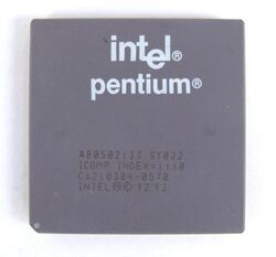
Intel Pentium P54 133 MHz - 3.3 million transistors
- 90 mm2 die size
- Family 5 model 2
- Variants
- Socket 5 296/320 pin PGA package
- 133 MHz, 218.9 MIPS (4.14 SPECint95, 3.12 SPECfp95 on Xpress 1MB L2)
- Introduced June 12, 1995
- 150, 166 MHz, 230 and 247 MIPS respectively
- Introduced January 4, 1996
- 133 MHz, 218.9 MIPS (4.14 SPECint95, 3.12 SPECfp95 on Xpress 1MB L2)
- Socket 7 296/321 pin PGA package
- 200 MHz, 270 MIPS (5.47 SPECint95, 3.68 SPECfp95)
- Introduced June 10, 1996
- 200 MHz, 270 MIPS (5.47 SPECint95, 3.68 SPECfp95)


Pentium with MMX Technology
- P55C – 0.35 μm process technology
- Introduced January 8, 1997
- Intel MMX (instruction set) support
- Socket 7 296/321 pin PGA (pin grid array) package
- 16 KB L1 instruction cache
- 16 KB L1 data cache
- 4.5 million transistors
- System bus clock rate 66 MHz
- Basic P55C is family 5 model 4, mobile are family 5 model 7 and 8
- Variants
- 166, 200 MHz introduced January 8, 1997
- 233 MHz introduced June 2, 1997
- 133 MHz (Mobile)
- 166, 266 MHz (Mobile) introduced January 12, 1998
- 200, 233 MHz (Mobile) introduced September 8, 1997
- 300 MHz (Mobile) introduced January 7, 1999

- Introduced November 1, 1995
- Multichip Module (2 die)
- Precursor to Pentium II and III
- Primarily used in server systems
- Socket 8 processor package (387 pins) (Dual SPGA)
- 5.5 million transistors
- Family 6 model 1
- 0.6 μm process technology
- 16 KB L1 cache
- 256 KB integrated L2 cache
- 60 MHz system bus clock rate
- Variants
- 150 MHz
- 0.35 μm process technology, (two die, a 0.35 μm CPU with 0.6 μm L2 cache)
- 5.5 million transistors
- 512 KB or 256 KB integrated L2 cache
- 60 or 66 MHz system bus clock rate
- Variants
- 150 MHz (60 MHz bus clock rate, 256 KB 0.5 μm cache) introduced November 1, 1995
- 166 MHz (66 MHz bus clock rate, 512 KB 0.35 μm cache) introduced November 1, 1995
- 180 MHz (60 MHz bus clock rate, 256 KB 0.6 μm cache) introduced November 1, 1995
- 200 MHz (66 MHz bus clock rate, 256 KB 0.6 μm cache) introduced November 1, 1995
- 200 MHz (66 MHz bus clock rate, 512 KB 0.35 μm cache) introduced November 1, 1995
- 200 MHz (66 MHz bus clock rate, 1 MB 0.35 μm cache) introduced August 18, 1997
- Introduced May 7, 1997
- Pentium Pro with MMX and improved 16-bit performance
- 242-pin Slot 1 (SEC) processor package
- Voltage identification pins
- 7.5 million transistors
- 32 KB L1 cache
- 512 KB 1⁄2 bandwidth external L2 cache
- The only Pentium II that did not have the L2 cache at 1⁄2 bandwidth of the core was the Pentium II 450 PE.
- Klamath – 0.35 μm process technology (233, 266, 300 MHz)
- 66 MHz system bus clock rate
- Family 6 model 3
- Variants
- 233, 266, 300 MHz introduced May 7, 1997
- Deschutes – 0.25 μm process technology (333, 350, 400, 450 MHz)
- Introduced January 26, 1998
- 66 MHz system bus clock rate (333 MHz variant), 100 MHz system bus clock rate for all subsequent models
- Family 6 model 5
- Variants
- 333 MHz introduced January 26, 1998
- 350, 400 MHz introduced April 15, 1998
- 450 MHz introduced August 24, 1998
- 233, 266 MHz (Mobile) introduced April 2, 1998
- 333 MHz Pentium II Overdrive processor for Socket 8 Introduced August 10, 1998
- 300 MHz (Mobile) introduced September 9, 1998
- 333 MHz (Mobile) introduced January 25, 1999
Celeron (Pentium II-based)
- Covington – 0.25 μm process technology
- Introduced April 15, 1998
- 242-pin Slot 1 SEPP (Single Edge Processor Package)
- 7.5 million transistors
- 66 MHz system bus clock rate
- Slot 1
- 32 KB L1 cache
- No L2 cache
- Variants
- 266 MHz introduced April 15, 1998
- 300 MHz introduced June 9, 1998
- Mendocino – 0.25 μm process technology
- Introduced August 24, 1998
- 242-pin Slot 1 SEPP (Single Edge Processor Package), Socket 370 PPGA package
- 19 million transistors
- 66 MHz system bus clock rate
- Slot 1, Socket 370
- 32 KB L1 cache
- 128 KB integrated cache
- Family 6 model 6
- Variants
- 300, 333 MHz introduced August 24, 1998
- 366, 400 MHz introduced January 4, 1999
- 433 MHz introduced March 22, 1999
- 466 MHz
- 500 MHz introduced August 2, 1999
- 533 MHz introduced January 4, 2000
- 266 MHz (Mobile)
- 300 MHz (Mobile)
- 333 MHz (Mobile) introduced April 5, 1999
- 366 MHz (Mobile)
- 400 MHz (Mobile)
- 433 MHz (Mobile)
- 450 MHz (Mobile) introduced February 14, 2000
- 466 MHz (Mobile)
- 500 MHz (Mobile) introduced February 14, 2000
Pentium II Xeon (chronological entry)
- Introduced June 29, 1998
- See main entry
- Katmai – 0.25 μm process technology
- Introduced February 26, 1999
- Improved PII, i.e. P6-based core, now including Streaming SIMD Extensions (SSE)
- 9.5 million transistors
- 512 KB (512 x 1024 B) 1⁄2 bandwidth L2 External cache
- 242-pin Slot 1 SECC2 (Single Edge Contact cartridge 2) processor package
- System Bus clock rate 100 MHz, 133 MHz (B-models)
- Slot 1
- Family 6 model 7
- Variants
- 450, 500 MHz introduced February 26, 1999
- 550 MHz introduced May 17, 1999
- 600 MHz introduced August 2, 1999
- 533, 600 MHz introduced (133 MHz bus clock rate) September 27, 1999
- Coppermine – 0.18 μm process technology
- Introduced October 25, 1999
- 28.1 million transistors
- 256 KB (512 x 1024 B) Advanced Transfer L2 cache (Integrated)
- 242-pin Slot-1 SECC2 (Single Edge Contact cartridge 2) processor package, 370-pin FC-PGA (Flip-chip pin grid array) package
- System Bus clock rate 100 MHz (E-models), 133 MHz (EB models)
- Slot 1, Socket 370
- Family 6 model 8
- Variants
- 500 MHz (100 MHz bus clock rate)
- 533 MHz
- 550 MHz (100 MHz bus clock rate)
- 600 MHz
- 600 MHz (100 MHz bus clock rate)
- 650 MHz (100 MHz bus clock rate) introduced October 25, 1999
- 667 MHz introduced October 25, 1999
- 700 MHz (100 MHz bus clock rate) introduced October 25, 1999
- 733 MHz introduced October 25, 1999
- 750, 800 MHz (100 MHz bus clock rate) introduced December 20, 1999
- 850 MHz (100 MHz bus clock rate) introduced March 20, 2000
- 866 MHz introduced March 20, 2000
- 933 MHz introduced May 24, 2000
- 1000 MHz introduced March 8, 2000 (not widely available at time of release)
- 1100 MHz
- 1133 MHz (first version recalled, later re-released)
- 400, 450, 500 MHz (Mobile) introduced October 25, 1999
- 600, 650 MHz (Mobile) introduced January 18, 2000
- 700 MHz (Mobile) introduced April 24, 2000
- 750 MHz (Mobile) introduced June 19, 2000
- 800, 850 MHz (Mobile) introduced September 25, 2000
- 900, 1000 MHz (Mobile) introduced March 19, 2001
- Tualatin – 0.13 μm process technology
- Introduced July 2001
- 28.1 million transistors
- 32 KB (32 x 1024 B) L1 cache
- 256 KB or 512 KB Advanced Transfer L2 cache (integrated)
- 370-pin FC-PGA2 (flip-chip pin grid array) package
- 133 MHz system bus clock rate
- Socket 370
- Family 6 model 11
- Variants
- 1133 MHz (256 KB L2)
- 1133 MHz (512 KB L2)
- 1200 MHz
- 1266 MHz (512 KB L2)
- 1333 MHz
- 1400 MHz (512 KB L2)
Pentium II Xeon and Pentium III Xeon
- PII Xeon
- Variants
- 400 MHz introduced June 29, 1998
- 450 MHz (512 KB L2 cache) introduced October 6, 1998
- 450 MHz (1 MB and 2 MB L2 cache) introduced January 5, 1999
- Variants
- PIII Xeon
- Introduced October 25, 1999
- 9.5 million transistors at 0.25 μm or 28 million at 0.18 μm
- L2 cache is 256 KB, 1 MB, or 2 MB Advanced Transfer Cache (Integrated)
- Processor Package Style is Single Edge Contact Cartridge (S.E.C.C.2) or SC330
- System Bus clock rate 133 MHz (256 KB L2 cache) or 100 MHz (1–2 MB L2 cache)
- System Bus width: 64 bits
- Addressable memory: 64 GB
- Used in two-way servers and workstations (256 KB L2) or 4- and 8-way servers (1–2 MB L2)
- Family 6 model 10
- Variants
- 500 MHz (0.25 μm process) introduced March 17, 1999
- 550 MHz (0.25 μm process) introduced August 23, 1999
- 600 MHz (0.18 μm process, 256 KB L2 cache) introduced October 25, 1999
- 667 MHz (0.18 μm process, 256 KB L2 cache) introduced October 25, 1999
- 733 MHz (0.18 μm process, 256 KB L2 cache) introduced October 25, 1999
- 800 MHz (0.18 μm process, 256 KB L2 cache) introduced January 12, 2000
- 866 MHz (0.18 μm process, 256 KB L2 cache) introduced April 10, 2000
- 933 MHz (0.18 μm process, 256 KB L2 cache)
- 1000 MHz (0.18 μm process, 256 KB L2 cache) introduced August 22, 2000
- 700 MHz (0.18 μm process, 1–2 MB L2 cache) introduced May 22, 2000
Celeron (Pentium III Coppermine-based)
- Coppermine-128, 0.18 μm process technology
- Introduced March, 2000
- Streaming SIMD Extensions (SSE)
- Socket 370, FC-PGA processor package
- 28.1 million transistors
- 66 MHz system bus clock rate, 100 MHz system bus clock rate from January 3, 2001
- 32 KB L1 cache
- 128 KB Advanced Transfer L2 cache
- Family 6 model 8
- Variants
- 533 MHz
- 566 MHz
- 600 MHz
- 633, 667, 700 MHz introduced June 26, 2000
- 733, 766 MHz introduced November 13, 2000
- 800 MHz introduced January 3, 2001
- 850 MHz introduced April 9, 2001
- 900 MHz introduced July 2, 2001
- 950, 1000, 1100 MHz introduced August 31, 2001
- 550 MHz (Mobile)
- 600, 650 MHz (Mobile) introduced June 19, 2000
- 700 MHz (Mobile) introduced September 25, 2000
- 750 MHz (Mobile) introduced March 19, 2001
- 800 MHz (Mobile)
- 850 MHz (Mobile) introduced July 2, 2001
- 600 MHz (LV Mobile)
- 500 MHz (ULV Mobile) introduced January 30, 2001
- 600 MHz (ULV Mobile)
XScale (chronological entry – non-x86 architecture)
- Introduced August 23, 2000
- See main entry
Pentium 4 (not 4EE, 4E, 4F), Itanium, P4-based Xeon, Itanium 2 (chronological entries)
- Introduced April 2000 – July 2002
- See main entries
Pentium III Tualatin-based
- Tualatin – 0.13 μm process technology
- 32 KB L1 cache
- 512KB Advanced Transfer L2 cache
- 133 MHz system bus clock rate
- Socket 370
- Variants
- 1.0 GHz
- 1.13 GHz
- 1.26 GHz
- 1.4 GHz
Celeron (Pentium III Tualatin-based)
- Tualatin Celeron – 0.13 μm process technology
- 32 KB L1 cache
- 256 KB Advanced Transfer L2 cache
- 100 MHz system bus clock rate
- Socket 370
- Family 6 model 11
- Variants
- 1.0 GHz
- 1.1 GHz
- 1.2 GHz
- 1.3 GHz
- 1.4 GHz
- Banias 0.13 μm process technology
- Introduced March 2003
- 64 KB L1 cache
- 1 MB L2 cache (integrated)
- Based on Pentium III core, with SSE2 SIMD instructions and deeper pipeline
- 77 million transistors
- Micro-FCPGA, Micro-FCBGA processor package
- Heart of the Intel mobile Centrino system
- 400 MHz Netburst-style system bus
- Family 6 model 9
- Variants
- 900 MHz (ultra low voltage)
- 1.0 GHz (ultra low voltage)
- 1.1 GHz (low voltage)
- 1.2 GHz (low voltage)
- 1.3 GHz
- 1.4 GHz
- 1.5 GHz
- 1.6 GHz
- 1.7 GHz
- Dothan 0.09 μm (90 nm) process technology
- Introduced May 2004
- 2 MB L2 cache
- 140 million transistors
- Revised data prefetch unit
- 400 MHz Netburst-style system bus
- 21W TDP
- Family 6 model 13
- Variants
- 1.00 GHz (Pentium M 723) (ultra low voltage, 5 W TDP)
- 1.10 GHz (Pentium M 733) (ultra low voltage, 5 W TDP)
- 1.20 GHz (Pentium M 753) (ultra low voltage, 5 W TDP)
- 1.30 GHz (Pentium M 718) (low voltage, 10 W TDP)
- 1.40 GHz (Pentium M 738) (low voltage, 10 W TDP)
- 1.50 GHz (Pentium M 758) (low voltage, 10 W TDP)
- 1.60 GHz (Pentium M 778) (low voltage, 10 W TDP)
- 1.40 GHz (Pentium M 710)
- 1.50 GHz (Pentium M 715)
- 1.60 GHz (Pentium M 725)
- 1.70 GHz (Pentium M 735)
- 1.80 GHz (Pentium M 745)
- 2.00 GHz (Pentium M 755)
- 2.10 GHz (Pentium M 765)
- Dothan 533 0.09 μm (90 nm) process technology
- Introduced Q1 2005
- Same as Dothan except with a 533 MHz NetBurst-style system bus and 27W TDP
- Variants
- 1.60 GHz (Pentium M 730)
- 1.73 GHz (Pentium M 740)
- 1.86 GHz (Pentium M 750)
- 2.00 GHz (Pentium M 760)
- 2.13 GHz (Pentium M 770)
- 2.26 GHz (Pentium M 780)
- Stealey 0.09 μm (90 nm) process technology
- Introduced Q2 2007
- 512 KB L2, 3 W TDP
- Variants
- 600 MHz (A100)
- 800 MHz (A110)
- Banias-512 0.13 μm process technology
- Dothan-1024 90 nm process technology
- 64 KB L1 cache
- 1 MB L2 cache (integrated)
- SSE2 SIMD instructions
- No SpeedStep technology, is not part of the 'Centrino' package
- Variants
- 350 – 1.30 GHz
- 350J – 1.30 GHz, with Execute Disable bit
- 360 – 1.40 GHz
- 360J – 1.40 GHz, with Execute Disable bit
- 370 – 1.50 GHz, with Execute Disable bit
- Family 6, Model 13, Stepping 8[7]
- 380 – 1.60 GHz, with Execute Disable bit
- 390 – 1.70 GHz, with Execute Disable bit
- Yonah-1024 65 nm process technology
- 64 KB L1 cache
- 1 MB L2 cache (integrated)
- SSE3 SIMD instructions, 533 MHz front-side bus, execute-disable bit
- No SpeedStep technology, is not part of the 'Centrino' package
- Variants
- 410 – 1.46 GHz
- 420 – 1.60 GHz,
- 423 – 1.06 GHz (ultra low voltage)
- 430 – 1.73 GHz
- 440 – 1.86 GHz
- 443 – 1.20 GHz (ultra low voltage)
- 450 – 2.00 GHz
- Yonah 0.065 μm (65 nm) process technology
- Introduced January 2006
- 533/667 MHz front side bus
- 2 MB (Shared on Duo) L2 cache
- SSE3 SIMD instructions
- 31W TDP (T versions)
- Family 6, Model 14
- Variants:
- Intel Core Duo T2700 2.33 GHz
- Intel Core Duo T2600 2.16 GHz
- Intel Core Duo T2500 2 GHz
- Intel Core Duo T2450 2 GHz
- Intel Core Duo T2400 1.83 GHz
- Intel Core Duo T2300 1.66 GHz
- Intel Core Duo T2050 1.6 GHz
- Intel Core Duo T2300e 1.66 GHz
- Intel Core Duo T2080 1.73 GHz
- Intel Core Duo L2500 1.83 GHz (low voltage, 15W TDP)
- Intel Core Duo L2400 1.66 GHz (low voltage, 15 W TDP)
- Intel Core Duo L2300 1.5 GHz (low voltage, 15 W TDP)
- Intel Core Duo U2500 1.2 GHz (ultra low voltage, 9 W TDP)
- Intel Core Solo T1350 1.86 GHz (533 FSB)
- Intel Core Solo T1300 1.66 GHz
- Intel Core Solo T1200 1.5 GHz[8]
Dual-Core Xeon LV
- Sossaman 0.065 μm (65 nm) process technology
- Introduced March 2006
- Based on Yonah core, with SSE3 SIMD instructions
- 667 MHz frontside bus
- 2 MB Shared L2 cache
- Variants
- 2.0 GHz
32-bit processors: NetBurst microarchitecture
- 0.18 μm process technology (1.40 and 1.50 GHz)
- 0.18 μm process technology (1.7 GHz)
- Introduced April 23, 2001
- See the 1.4 and 1.5 chips for details
- 0.18 μm process technology (1.6 and 1.8 GHz)
- Introduced July 2, 2001
- See 1.4 and 1.5 chips for details
- Core Voltage is 1.15 volts in Maximum Performance Mode; 1.05 volts in Battery Optimized Mode
- Power <1 watt in Battery Optimized Mode
- Used in full-size and then light mobile PCs
- 0.18 μm process technology Willamette (1.9 and 2.0 GHz)
- Introduced August 27, 2001
- See 1.4 and 1.5 chips for details
- Family 15 model 1
- Pentium 4 (2 GHz, 2.20 GHz)
- Introduced January 7, 2002
- Pentium 4 (2.4 GHz)
- Introduced April 2, 2002
- 0.13 μm process technology Northwood A (1.7, 1.8, 1.9, 2, 2.2, 2.4, 2.5, 2.6, 2.8 (OEM), 3.0 (OEM) GHz)
- Improved branch prediction and other microcodes tweaks
- 512 KB integrated L2 cache
- 55 million transistors
- 400 MHz system bus
- Family 15 model 2
- 0.13 μm process technology Northwood B (2.26, 2.4, 2.53, 2.66, 2.8, 3.06 GHz)
- 533 MHz system bus. (3.06 includes Intel's Hyper-Threading technology)
- 0.13 μm process technology Northwood C (2.4, 2.6, 2.8, 3.0, 3.2, 3.4 GHz)
- 800 MHz system bus (all versions include Hyper-Threading)
- 6500 to 10,000 MIPS
Itanium (chronological entry – new non-x86 architecture)
- Introduced 2001
- See main entry
Xeon (32-bit NetBurst)
- Official designation now Xeon, i.e. not "Pentium 4 Xeon"
- Xeon 1.4, 1.5, 1.7 GHz
- Introduced May 21, 2001
- L2 cache was 256 KB Advanced Transfer Cache (Integrated)
- Processor Package Style was Organic Land Grid Array 603 (OLGA 603)
- System Bus clock rate 400 MHz
- SSE2 SIMD Extensions
- Used in high-performance and mid-range dual processor enabled workstations
- Xeon 2.0 GHz and up to 3.6 GHz
- Introduced September 25, 2001
Itanium 2 (chronological entry – new non-x86 architecture)
- Introduced July 2002
- See main entry
Mobile Pentium 4-M
- 0.13 μm process technology
- 55 million transistors
- 512 KB L2 cache
- BUS a 400 MHz
- Supports up to 1 GB of DDR 266 MHz memory
- Supports ACPI 2.0 and APM 1.2 System Power Management
- 1.3–1.2 V (SpeedStep)
- Power: 1.2 GHz 20.8 W, 1.6 GHz 30 W, 2.6 GHz 35 W
- Sleep Power 5 W (1.2 V)
- Deeper Sleep Power = 2.9 W (1.0 V)
- 1.40 GHz – 23 April 2002
- 1.50 GHz – 23 April 2002
- 1.60 GHz – 4 March 2002
- 1.70 GHz – 4 March 2002
- 1.80 GHz – 23 April 2002
- 1.90 GHz – 24 June 2002
- 2.00 GHz – 24 June 2002
- 2.20 GHz – 16 September 2002
- 2.40 GHz – 14 January 2003
- 2.50 GHz – 16 April 2003
- 2.60 GHz – 11 June 2003
Pentium 4 EE
- Introduced September 2003
- EE = "Extreme Edition"
- Built from the Xeon's "Gallatin" core, but with 2 MB cache
Pentium 4E
- Introduced February 2004
- built on 0.09 μm (90 nm) process technology Prescott (2.4 A, 2.8, 2.8 A, 3.0, 3.2, 3.4, 3.6, 3.8 ) 1 MB L2 cache
- 533 MHz system bus (2.4A and 2.8A only)
- 800 MHz system bus (all other models)
- 125 million transistors in 1 MB Models
- 169 million transistors in 2 MB Models
- Hyper-Threading support is only available on CPUs using the 800 MHz system bus.
- The processor's integer instruction pipeline has been increased from 20 stages to 31 stages, which theoretically allows for even greater bandwidth
- 7500 to 11,000 MIPS
- LGA 775 versions are in the 5xx series (32-bit) and 5x1 series (with Intel 64)
- The 6xx series has 2 MB L2 cache and Intel 64
- New instruction set, not at all related to x86
- Before the feature was eliminated (Montecito, July 2006) IA-64 processors supported 32-bit x86 in hardware, but slowly (see its 2001 market reception and 2006 architectural changes)[dubious ]
Itanium
- Code name Merced
- Family 7
- Released May 29, 2001
- 733 MHz and 800 MHz
- 2 MB cache
- All recalled and replaced by Itanium 2
Itanium 2
- Family 0x1F
- Released July 2002
- 900 MHz – 1.6 GHz
- McKinley 900 MHz 1.5 MB cache, Model 0x0
- McKinley 1 GHz, 3 MB cache, Model 0x0
- Deerfield 1 GHz, 1.5 MB cache, Model 0x1
- Madison 1.3 GHz, 3 MB cache, Model 0x1
- Madison 1.4 GHz, 4 MB cache, Model 0x1
- Madison 1.5 GHz, 6 MB cache, Model 0x1
- Madison 1.67 GHz, 9 MB cache, Model 0x1
- Hondo 1.4 GHz, 4 MB cache, dual-core MCM, Model 0x1
64-bit processors: Intel 64 – NetBurst microarchitecture
- Intel Extended Memory 64 Technology
- Mostly compatible with AMD's AMD64 architecture
- Introduced Spring 2004, with the Pentium 4F (D0 and later P4 steppings)
Pentium 4F
- Prescott-2M built on 0.09 μm (90 nm) process technology
- 2.8–3.8 GHz (model numbers 6x0)
- Introduced February 20, 2005
- Same features as Prescott with the addition of:
- Cedar Mill built on 0.065 μm (65 nm) process technology
- 3.0–3.6 GHz (model numbers 6x1)
- Introduced January 16, 2006
- Die shrink of Prescott-2M
- Same features as Prescott-2M
- Family 15 Model 4
- Dual-core microprocessor
- No Hyper-Threading
- 800 (4×200) MHz front side bus
- LGA 775 (Socket T)
- Smithfield (Pentium D) – 90 nm process technology (2.66–3.2 GHz)
- Introduced May 26, 2005
- 2.66–3.2 GHz (model numbers 805–840)
- 230 million transistors
- 1 MB × 2 (non-shared, 2 MB total) L2 cache
- Cache coherency between cores requires communication over the FSB
- Performance increase of 60% over similarly clocked Prescott
- 2.66 GHz (533 MHz FSB) Pentium D 805 introduced December 2005
- Contains 2x Prescott dies in one package
- Family 15 Model 4
- Presler (Pentium D) – 65 nm process technology (2.8–3.6 GHz)
- Introduced January 16, 2006
- 2.8–3.6 GHz (model numbers 915–960)
- 376 million transistors
- 2× 2 MB (non-shared, 4 MB total) L2 cache
- Contains 2x Cedar Mill dies in one package
- Variants
- Pentium D 945
Pentium Extreme Edition
- Dual-core microprocessor
- Enabled Hyper-Threading
- 800 (4×200) MHz front side bus
- Smithfield (Pentium Extreme Edition) – 90 nm process technology (3.2 GHz)
- Variants
- Pentium 840 EE – 3.20 GHz (2 × 1 MB L2)
- Variants
- Presler (Pentium Extreme Edition) – 65 nm process technology (3.46, 3.73)
- 2 MB × 2 (non-shared, 4 MB total) L2 cache
- Variants
- Pentium 955 EE – 3.46 GHz, 1066 MHz front side bus
- Pentium 965 EE – 3.73 GHz, 1066 MHz front side bus
- Pentium 969 EE – 3.73 GHz, 1066 MHz front side bus
Xeon (64-bit NetBurst)
- Nocona
- Introduced 2004
- Irwindale
- Introduced 2004
- Cranford
- Introduced April 2005
- MP version of Nocona
- Potomac
- Introduced April 2005
- Cranford with 8 MB of L3 cache
- Paxville DP (2.8 GHz)
- Introduced October 10, 2005
- Dual-core version of Irwindale, with 4 MB of L2 cache (2 MB per core)
- 2.8 GHz
- 800 MT/s front side bus
- Paxville MP – 90 nm process (2.67 – 3.0 GHz)
- Introduced November 1, 2005
- Dual-core Xeon 7000 series
- MP-capable version of Paxville DP
- 2 MB of L2 cache (1 MB per core) or 4 MB of L2 (2 MB per core)
- 667 MT/s FSB or 800 MT/s FSB
- Dempsey – 65 nm process (2.67 – 3.73 GHz)
- Introduced May 23, 2006
- Dual-core Xeon 5000 series
- MP version of Presler
- 667 MT/s or 1066 MT/s FSB
- 4 MB of L2 cache (2 MB per core)
- LGA 771 (Socket J).
- Tulsa – 65 nm process (2.5 – 3.4 GHz)
- Introduced August 29, 2006
- Dual-core Xeon 7100-series
- Improved version of Paxville MP
- 667 MT/s or 800 MT/s FSB
64-bit processors: Intel 64 – Core microarchitecture
Xeon (64-bit Core microarchitecture)
- Woodcrest – 65 nm process technology
- Server and Workstation CPU (SMP support for dual CPU system)
- Introduced June 26, 2006
- Intel VT-x, multiple OS support
- EIST (Enhanced Intel SpeedStep Technology) in 5140, 5148LV, 5150, 5160
- Execute Disable Bit
- TXT, enhanced security hardware extensions
- SSSE3 SIMD instructions
- iAMT2 (Intel Active Management Technology), remotely manage computers
- Variants
- Xeon 5160 – 3.00 GHz (4 MB L2, 1333 MHz FSB, 80 W)
- Xeon 5150 – 2.66 GHz (4 MB L2, 1333 MHz FSB, 65 W)
- Xeon 5140 – 2.33 GHz (4 MB L2, 1333 MHz FSB, 65 W)
- Xeon 5130 – 2.00 GHz (4 MB L2, 1333 MHz FSB, 65 W)
- Xeon 5120 – 1.86 GHz (4 MB L2, 1066 MHz FSB, 65 W)
- Xeon 5110 – 1.60 GHz (4 MB L2, 1066 MHz FSB, 65 W)
- Xeon 5148LV – 2.33 GHz (4 MB L2, 1333 MHz FSB, 40 W) (low voltage edition)
- Clovertown – 65 nm process technology
- Server and Workstation CPU (SMP support for dual CPU system)
- Introduced December 13, 2006
- Quad-core
- Intel VT-x, multiple OS support
- EIST (Enhanced Intel SpeedStep Technology) in E5365, L5335
- Execute Disable Bit
- TXT, enhanced security hardware extensions
- SSSE3 SIMD instructions
- iAMT2 (Intel Active Management Technology), remotely manage computers
- Variants
- Xeon X5355 – 2.66 GHz (2×4 MB L2, 1333 MHz FSB, 105 W)
- Xeon E5345 – 2.33 GHz (2×4 MB L2, 1333 MHz FSB, 80 W)
- Xeon E5335 – 2.00 GHz (2×4 MB L2, 1333 MHz FSB, 80 W)
- Xeon E5320 – 1.86 GHz (2×4 MB L2, 1066 MHz FSB, 65 W)
- Xeon E5310 – 1.60 GHz (2×4 MB L2, 1066 MHz FSB, 65 W)
- Xeon L5320 – 1.86 GHz (2×4 MB L2, 1066 MHz FSB, 50 W) (low voltage edition)
- Conroe – 65 nm process technology
- Desktop CPU (SMP support restricted to 2 CPUs)
- Two cores on one die
- Introduced July 27, 2006
- SSSE3 SIMD instructions
- 291 million transistors
- 64 KB of L1 cache per core (32+32 KB 8-way)
- Intel VT-x, multiple OS support
- TXT, enhanced security hardware extensions
- Execute Disable Bit
- EIST (Enhanced Intel SpeedStep Technology)
- iAMT2 (Intel Active Management Technology), remotely manage computers
- Intel Management Engine introduced
- LGA 775
- Variants
- Core 2 Duo E6850 – 3.00 GHz (4 MB L2, 1333 MHz FSB)
- Core 2 Duo E6800 – 2.93 GHz (4 MB L2, 1066 MHz FSB)
- Core 2 Duo E6750 – 2.67 GHz (4 MB L2, 1333 MHz FSB, 65W)
- Core 2 Duo E6700 – 2.67 GHz (4 MB L2, 1066 MHz FSB)
- Core 2 Duo E6600 – 2.40 GHz (4 MB L2, 1066 MHz FSB, 65W)
- Core 2 Duo E6550 – 2.33 GHz (4 MB L2, 1333 MHz FSB)
- Core 2 Duo E6420 – 2.13 GHz (4 MB L2, 1066 MHz FSB)
- Core 2 Duo E6400 – 2.13 GHz (2 MB L2, 1066 MHz FSB)
- Core 2 Duo E6320 – 1.86 GHz (4 MB L2, 1066 MHz FSB) Family 6, Model 15, Stepping 6
- Core 2 Duo E6300 – 1.86 GHz (2 MB L2, 1066 MHz FSB)
- Conroe XE – 65 nm process technology
- Desktop Extreme Edition CPU (SMP support restricted to 2 CPUs)
- Introduced July 27, 2006
- same features as Conroe
- LGA 775
- Variants
- Core 2 Extreme X6800 – 2.93 GHz (4 MB L2, 1066 MHz FSB)
- Allendale (Intel Core 2) – 65 nm process technology
- Desktop CPU (SMP support restricted to 2 CPUs)
- Two CPUs on one die
- Introduced January 21, 2007
- SSSE3 SIMD instructions
- 167 million transistors
- TXT, enhanced security hardware extensions
- Execute Disable Bit
- EIST (Enhanced Intel SpeedStep Technology)
- iAMT2 (Intel Active Management Technology), remotely manage computers
- LGA 775
- Variants
- Core 2 Duo E4700 – 2.60 GHz (2 MB L2, 800 MHz FSB)
- Core 2 Duo E4600 – 2.40 GHz (2 MB L2, 800 MHz FSB)
- Core 2 Duo E4500 – 2.20 GHz (2 MB L2, 800 MHz FSB)
- Core 2 Duo E4400 – 2.00 GHz (2 MB L2, 800 MHz FSB)
- Core 2 Duo E4300 – 1.80 GHz (2 MB L2, 800 MHz FSB) Family 6, Model 15, Stepping 2
- Merom – 65 nm process technology
- Mobile CPU (SMP support restricted to 2 CPUs)
- Introduced July 27, 2006
- Family 6, Model 15
- same features as Conroe
- Socket M / Socket P
- Variants
- Core 2 Duo T7800 – 2.60 GHz (4 MB L2, 800 MHz FSB) (Santa Rosa platform)
- Core 2 Duo T7700 – 2.40 GHz (4 MB L2, 800 MHz FSB)
- Core 2 Duo T7600 – 2.33 GHz (4 MB L2, 667 MHz FSB)
- Core 2 Duo T7500 – 2.20 GHz (4 MB L2, 800 MHz FSB)
- Core 2 Duo T7400 – 2.16 GHz (4 MB L2, 667 MHz FSB)
- Core 2 Duo T7300 – 2.00 GHz (4 MB L2, 800 MHz FSB)
- Core 2 Duo T7250 – 2.00 GHz (2 MB L2, 800 MHz FSB)
- Core 2 Duo T7200 – 2.00 GHz (4 MB L2, 667 MHz FSB)
- Core 2 Duo T7100 – 1.80 GHz (2 MB L2, 800 MHz FSB)
- Core 2 Duo T5600 – 1.83 GHz (2 MB L2, 667 MHz FSB) Family 6, Model 15, Stepping 6
- Core 2 Duo T5550 – 1.83 GHz (2 MB L2, 667 MHz FSB, no VT)
- Core 2 Duo T5500 – 1.66 GHz (2 MB L2, 667 MHz FSB, no VT)
- Core 2 Duo T5470 – 1.60 GHz (2 MB L2, 800 MHz FSB, no VT) Family 6, Model 15, Stepping 13
- Core 2 Duo T5450 – 1.66 GHz (2 MB L2, 667 MHz FSB, no VT)
- Core 2 Duo T5300 – 1.73 GHz (2 MB L2, 533 MHz FSB, no VT)
- Core 2 Duo T5270 – 1.40 GHz (2 MB L2, 800 MHz FSB, no VT)
- Core 2 Duo T5250 – 1.50 GHz (2 MB L2, 667 MHz FSB, no VT)
- Core 2 Duo T5200 – 1.60 GHz (2 MB L2, 533 MHz FSB, no VT)
- Core 2 Duo L7500 – 1.60 GHz (4 MB L2, 800 MHz FSB) (low voltage)
- Core 2 Duo L7400 – 1.50 GHz (4 MB L2, 667 MHz FSB) (low voltage)
- Core 2 Duo L7300 – 1.40 GHz (4 MB L2, 800 MHz FSB) (low voltage)
- Core 2 Duo L7200 – 1.33 GHz (4 MB L2, 667 MHz FSB) (low voltage)
- Core 2 Duo U7700 – 1.33 GHz (2 MB L2, 533 MHz FSB) (ultra low voltage)
- Core 2 Duo U7600 – 1.20 GHz (2 MB L2, 533 MHz FSB) (ultra low voltage)
- Core 2 Duo U7500 – 1.06 GHz (2 MB L2, 533 MHz FSB) (ultra low voltage)
- Kentsfield – 65 nm process technology
- Two dual-core CPU dies in one package
- Desktop CPU quad-core (SMP support restricted to 4 CPUs)
- Introduced December 13, 2006
- same features as Conroe but with 4 CPU cores
- 586 million transistors
- LGA 775
- Family 6, Model 15, Stepping 11
- Variants
- Core 2 Extreme QX6850 – 3 GHz (2×4 MB L2 cache, 1333 MHz FSB)
- Core 2 Extreme QX6800 – 2.93 GHz (2×4 MB L2 cache, 1066 MHz FSB) (April 9, 2007)
- Core 2 Extreme QX6700 – 2.66 GHz (2×4 MB L2 cache, 1066 MHz FSB) (November 14, 2006)
- Core 2 Quad Q6700 – 2.66 GHz (2×4 MB L2 cache, 1066 MHz FSB) (July 22, 2007)
- Core 2 Quad Q6600 – 2.40 GHz (2×4 MB L2 cache, 1066 MHz FSB) (January 7, 2007)
- Wolfdale – 45 nm process technology
- Die shrink of Conroe
- Same features as Conroe with the addition of:
- 410 million transistors
- Variants
- Core 2 Duo E8600 – 3.33 GHz (6 MB L2, 1333 MHz FSB)
- Core 2 Duo E8500 – 3.16 GHz (6 MB L2, 1333 MHz FSB)
- Core 2 Duo E8435 – 3.07 GHz (6 MB L2, 1066 MHz FSB)
- Core 2 Duo E8400 – 3.00 GHz (6 MB L2, 1333 MHz FSB)
- Core 2 Duo E8335 – 2.93 GHz (6 MB L2, 1066 MHz FSB)
- Core 2 Duo E8300 – 2.83 GHz (6 MB L2, 1333 MHz FSB)
- Core 2 Duo E8235 – 2.80 GHz (6 MB L2, 1066 MHz FSB)
- Core 2 Duo E8200 – 2.66 GHz (6 MB L2, 1333 MHz FSB)
- Core 2 Duo E8135 – 2.66 GHz (6 MB L2, 1066 MHz FSB)
- Core 2 Duo E8190 – 2.66 GHz (6 MB L2, 1333 MHz FSB, no TXT, no VT)
- Wolfdale-3M (Intel Core 2) – 45 nm process technology
- Intel Trusted Execution Technology
- Variants
- Core 2 Duo E7600 – 3.06 GHz (3 MB L2, 1066 MHz FSB)
- Core 2 Duo E7500 – 2.93 GHz (3 MB L2, 1066 MHz FSB)
- Core 2 Duo E7400 – 2.80 GHz (3 MB L2, 1066 MHz FSB)
- Core 2 Duo E7300 – 2.66 GHz (3 MB L2, 1066 MHz FSB)
- Core 2 Duo E7200 – 2.53 GHz (3 MB L2, 1066 MHz FSB)
- Yorkfield – 45 nm process technology
- Quad-core CPU
- Die shrink of Kentsfield
- Contains 2x Wolfdale dual-core dies in one package
- Same features as Wolfdale
- 820 million transistors
- Variants
- Core 2 Extreme QX9770 – 3.20 GHz (2×6 MB L2, 1600 MHz FSB)
- Core 2 Extreme QX9650 – 3.00 GHz (2×6 MB L2, 1333 MHz FSB)
- Core 2 Quad Q9705 – 3.16 GHz (2×3 MB L2, 1333 MHz FSB)
- Core 2 Quad Q9700 – 3.16 GHz (2×3 MB L2, 1333 MHz FSB)
- Core 2 Quad Q9650 – 3 GHz (2×6 MB L2, 1333 MHz FSB)
- Core 2 Quad Q9550 – 2.83 GHz (2×6 MB L2, 1333 MHz FSB, 95 W TDP)
- Core 2 Quad Q9550s – 2.83 GHz (2×6 MB L2, 1333 MHz FSB, 65 W TDP)
- Core 2 Quad Q9450 – 2.66 GHz (2×6 MB L2, 1333 MHz FSB, 95 W TDP)
- Core 2 Quad Q9505 – 2.83 GHz (2×3 MB L2, 1333 MHz FSB, 95 W TDP)
- Core 2 Quad Q9505s – 2.83 GHz (2×3 MB L2, 1333 MHz FSB, 65 W TDP)
- Core 2 Quad Q9500 – 2.83 GHz (2×3 MB L2, 1333 MHz FSB, 95 W TDP, no TXT)
- Core 2 Quad Q9400 – 2.66 GHz (2×3 MB L2, 1333 MHz FSB, 95 W TDP)
- Core 2 Quad Q9400s – 2.66 GHz (2×3 MB L2, 1333 MHz FSB, 65 W TDP)
- Core 2 Quad Q9300 – 2.50 GHz (2×3 MB L2, 1333 MHz FSB, 95 W TDP)
- Core 2 Quad Q8400 – 2.66 GHz (2×2 MB L2, 1333 MHz FSB, 95 W TDP)
- Core 2 Quad Q8400s – 2.66 GHz (2×2 MB L2, 1333 MHz FSB, 65 W TDP)
- Core 2 Quad Q8300 – 2.50 GHz (2×2 MB L2, 1333 MHz FSB, 95 W TDP)
- Core 2 Quad Q8300s – 2.50 GHz (2×2 MB L2, 1333 MHz FSB, 65 W TDP)
- Core 2 Quad Q8200 – 2.33 GHz (2×2 MB L2, 1333 MHz FSB, 95 W TDP)
- Core 2 Quad Q8200s – 2.33 GHz (2×2 MB L2, 1333 MHz FSB, 65 W TDP)
- Core 2 Quad Q7600 – 2.70 GHz (2×1 MB L2, 800 MHz FSB, no SSE4) (no Q7600 listed here)
- Intel Core2 Quad Mobile processor family – 45 nm process technology
- Quad-core CPU
- Variants
- Core 2 Quad Q9100 – 2.26 GHz (2×6 MB L2, 1066 MHz FSB, 45 W TDP)
- Core 2 Quad Q9000 – 2.00 GHz (2×3 MB L2, 1066 MHz FSB, 45 W TDP)
Intel Pentium Dual-Core
- Allendale (Pentium Dual-Core) – 65 nm process technology
- Desktop CPU (SMP support restricted to 2 CPUs)
- Two cores on one die
- Introduced January 21, 2007
- SSSE3 SIMD instructions
- 167 million transistors
- TXT, enhanced security hardware extensions
- Execute Disable Bit
- EIST (Enhanced Intel SpeedStep Technology)
- Variants
- Intel Pentium E2220 – 2.40 GHz (1 MB L2, 800 MHz FSB)
- Intel Pentium E2200 – 2.20 GHz (1 MB L2, 800 MHz FSB)
- Intel Pentium E2180 – 2.00 GHz (1 MB L2, 800 MHz FSB)
- Intel Pentium E2160 – 1.80 GHz (1 MB L2, 800 MHz FSB)
- Intel Pentium E2140 – 1.60 GHz (1 MB L2, 800 MHz FSB)
- Wolfdale-3M (Pentium Dual-Core) – 45 nm process technology
- Intel Pentium E6800 – 3.33 GHz (2 MB L2,1066 MHz FSB)
- Intel Pentium E6700 – 3.20 GHz (2 MB L2,1066 MHz FSB)
- Intel Pentium E6600 – 3.06 GHz (2 MB L2,1066 MHz FSB)
- Intel Pentium E6500 – 2.93 GHz (2 MB L2,1066 MHz FSB)
- Intel Pentium E6300 – 2.80 GHz (2 MB L2,1066 MHz FSB)
- Intel Pentium E5800 – 3.20 GHz (2 MB L2, 800 MHz FSB)
- Intel Pentium E5700 – 3.00 GHz (2 MB L2, 800 MHz FSB)
- Intel Pentium E5500 – 2.80 GHz (2 MB L2, 800 MHz FSB)
- Intel Pentium E5400 – 2.70 GHz (2 MB L2, 800 MHz FSB)
- Intel Pentium E5300 – 2.60 GHz (2 MB L2, 800 MHz FSB)
- Intel Pentium E5200 – 2.50 GHz (2 MB L2, 800 MHz FSB)
- Intel Pentium E2210 – 2.20 GHz (1 MB L2, 800 MHz FSB)
Celeron (64-bit Core microarchitecture)
- Allendale (Celeron, 64-bit Core microarchitecture) – 65 nm process technology
- Variants
- Intel Celeron E1600 – 2.40 GHz (512 KB L2, 800 MHz FSB)
- Intel Celeron E1500 – 2.20 GHz (512 KB L2, 800 MHz FSB)
- Intel Celeron E1400 – 2.00 GHz (512 KB L2, 800 MHz FSB)
- Intel Celeron E1300 – 1.80 GHz (512 KB L2, 800 MHz FSB) (does it exist?)[citation needed]
- Intel Celeron E1200 – 1.60 GHz (512 KB L2, 800 MHz FSB)
- Variants
- Wolfdale-3M (Celeron, 64-bit Core microarchitecture) – 45 nm process technology
- Variants
- Intel Celeron E3500 – 2.70 GHz (1 MB L2, 800 MHz FSB)
- Intel Celeron E3400 – 2.60 GHz (1 MB L2, 800 MHz FSB)
- Intel Celeron E3300 – 2.50 GHz (1 MB L2, 800 MHz FSB)
- Intel Celeron E3200 – 2.40 GHz (1 MB L2, 800 MHz FSB)
- Variants
- Conroe-L (Celeron, 64-bit Core microarchitecture) – 65 nm process technology
- Variants
- Intel Celeron 450 – 2.20 GHz (512 KB L2, 800 MHz FSB)
- Intel Celeron 440 – 2.00 GHz (512 KB L2, 800 MHz FSB)
- Intel Celeron 430 – 1.80 GHz (512 KB L2, 800 MHz FSB)
- Intel Celeron 420 – 1.60 GHz (512 KB L2, 800 MHz FSB)
- Intel Celeron 220 – 1.20 GHz (512 KB L2, 533 MHz FSB)
- Variants
- Conroe-CL (Celeron, 64-bit Core microarchitecture) – 65 nm process technology
- LGA 771 package
- Variants
- Intel Celeron 445 – 1.87 GHz (512 KB L2, 1066 MHz FSB)
Celeron M (64-bit Core microarchitecture)
- Merom-L 65 nm process technology
- 667 MHz FSB
- 575 – 2.00 GHz
- 585 – 2.16 GHz
64-bit processors: Intel 64 – Nehalem microarchitecture
Intel Pentium (Nehalem)
- Clarkdale (Pentium, Nehalem microarchitecture) – 32 nm process technology (manufacturing 7 Jan 2010)
- 2 physical cores/2 threads
- 32+32 KB L1 cache
- 256 KB L2 cache
- 3 MB L3 cache
- Introduced January 2010
- Socket 1156 LGA
- 2-channel DDR3
- Integrated HD GPU
- Variants
- G6950 – 2.8 GHz (no Hyper-Threading)[9]
- G6960 – 2.933 GHz (no Hyper-Threading)
Core i3 (1st Generation)
- Clarkdale (Core i3 1st Generation) – 32 nm process technology
- 2 physical cores/4 threads
- 32+32 KB L1 cache
- 256 KB L2 cache
- 4 MB L3 cache
- Introduced on January 7, 2010
- Socket 1156 LGA
- 2-channel DDR3
- Integrated HD GPU
- Variants
- 530 – 2.93 GHz Hyper-Threading
- 540 – 3.06 GHz Hyper-Threading
- 550 – 3.2 GHz Hyper-Threading
- 560 – 3.33 GHz Hyper-Threading
Core i5 (1st Generation)
- Lynnfield (Core i5 1st Generation) – 45 nm process technology
- 4 physical cores/4 threads
- 32+32 KB L1 cache
- 256 KB L2 cache
- 8 MB L3 cache
- Introduced September 8, 2009
- Family 6 Model E (Ext. Model 1E)
- Socket 1156 LGA
- 2-channel DDR3
- Variants
- 750S – 2.40 GHz/3.20 GHz Turbo Boost
- 750 – 2.66 GHz/3.20 GHz Turbo Boost
- 760 – 2.80 GHz/3.33 GHz Turbo Boost
- Clarkdale (Core i5 1st Generation) – 32 nm process technology
- 2 physical cores/4 threads
- 32+32 KB L1 cache
- 256 KB L2 cache
- 4 MB L3 cache
- Introduced January, 2010
- Socket 1156 LGA
- 2-channel DDR3
- Integrated HD GPU
- AES Support
- Variants
- 650/655K – 3.2 GHz Hyper-Threading Turbo Boost
- 660/661 – 3.33 GHz Hyper-Threading Turbo Boost
- 670 – 3.46 GHz Hyper-Threading Turbo Boost
- 680 – 3.60 GHz Hyper-Threading Turbo Boost
Core i7 (1st Generation)
- Bloomfield (Core i7 1st Generation) – 45 nm process technology
- 4 physical cores/8 threads
- 256 KB L2 cache
- 8 MB L3 cache
- Front side bus replaced with QuickPath up to 6.4 GT/s
- Hyper-Threading is again included. This had previously been removed at the introduction of Core line
- 781 million transistors
- Intel Turbo Boost Technology
- TDP 130W
- Introduced November 17, 2008
- Socket 1366 LGA
- 3-channel DDR3
- Variants
- 975 (extreme edition) – 3.33 GHz/3.60 GHz Turbo Boost
- 965 (extreme edition) – 3.20 GHz/3.46 GHz Turbo Boost
- 960 – 3.20 GHz/3.46 GHz Turbo Boost
- 950 – 3.06 GHz/3.33 GHz Turbo Boost
- 940 – 2.93 GHz/3.20 GHz Turbo Boost
- 930 – 2.80 GHz/3.06 GHz Turbo Boost
- 920 – 2.66 GHz/2.93 GHz Turbo Boost
- Lynnfield (Core i7 1st Generation) – 45 nm process technology
- 4 physical cores/8 threads
- 32+32 KB L1 cache
- 256 KB L2 cache
- 8 MB L3 cache
- No QuickPath, instead compatible with slower DMI interface
- Hyper-Threading is included
- Introduced September 8, 2009
- Socket 1156 LGA
- 2-channel DDR3
- Variants
- 880 – 3.06 GHz/3.73 GHz Turbo Boost (TDP 95W)
- 870/875K – 2.93 GHz/3.60 GHz Turbo Boost (TDP 95W)
- 870S – 2.67 GHz/3.60 GHz Turbo Boost (TDP 82W)
- 860 – 2.80 GHz/3.46 GHz Turbo Boost (TDP 95W)
- 860S – 2.53 GHz/3.46 GHz Turbo Boost (TDP 82W)
TODO: Westmere
- Gulftown – 32 nm process technology
- 6 physical cores
- 256 KB L2 cache
- 12 MB L3 cache
- Front side bus replaced with QuickPath up to 6.4 GT/s
- Hyper-Threading is included
- Intel Turbo Boost Technology
- Socket 1366 LGA
- TDP 130W
- Introduced 16 March 2010
- Variants
- 990X Extreme Edition – 3.46 GHz/3.73 GHz Turbo Boost
- 980X Extreme Edition – 3.33 GHz/3.60 GHz Turbo Boost
- 970 – 3.20 GHz/3.46 GHz Turbo Boost
- Clarksfield – Intel Core i7 Mobile processor family – 45 nm process technology
- 4 physical cores
- Hyper-Threading is included
- Intel Turbo Boost Technology
- Variants
- 940XM Extreme Edition – 2.13 GHz/3.33 GHz Turbo Boost (8 MB L3, TDP 55W)
- 920XM Extreme Edition – 2.00 GHz/3.20 GHz Turbo Boost (8 MB L3, TDP 55W)
- 840QM – 1.86 GHz/3.20 GHz Turbo Boost (8 MB L3, TDP 45W)
- 820QM – 1.73 GHz/3.06 GHz Turbo Boost (8 MB L3, TDP 45W)
- 740QM – 1.73 GHz/2.93 GHz Turbo Boost (6 MB L3, TDP 45W)
- 720QM – 1.60 GHz/2.80 GHz Turbo Boost (6 MB L3, TDP 45W)
Xeon (Nehalem Microarchitecture)
- Gainestown – 45 nm process technology
- Same processor dies as Bloomfield
- 256 KB L2 cache
- 8 MB L3 cache, 4 MB may be disabled
- QuickPath up to 6.4 GT/s
- Hyper-Threading is included in some models
- 781 million transistors
- Introduced March 29, 2009
- Variants
- W5590, X5570, X5560, X5550, E5540, E5530, L5530, E5520, L5520, L5518 – 4 cores, 8 MB L3 cache, HT
- E5506, L5506, E5504 – 4 cores, 4 MB L3 cache, no HT
- L5508, E5502, E5502 – 2 cores, 4 MB L3 cache, no HT
64-bit processors: Intel 64 – Sandy Bridge / Ivy Bridge microarchitecture
Celeron (Sandy Bridge/Ivy Bridge Microarchitecture)
- Sandy Bridge (Celeron-branded) – 32 nm process technology
- 2 physical cores/2 threads (500 series), 1 physical core/1 thread (model G440) or 1 physical core/2 threads (models G460 & G465)
- 2 MB L3 cache (500 series), 1 MB (model G440) or 1.5 MB (models G460 & G465)
- Introduced 3rd quarter, 2011
- Socket 1155 LGA
- 2-channel DDR3-1066
- 400 series has max TDP of 35 W
- 500-series variants ending in 'T' have a peak TDP of 35 W, others – 65 W
- Integrated GPU
- All variants have peak GPU turbo frequencies of 1 GHz
- Variants in the 400 series have GPUs running at a base frequency of 650 MHz
- Variants in the 500 series ending in 'T' have GPUs running at a base frequency of 650 MHz; others at 850 MHz
- All variants have 6 GPU execution units
- Variants
- G440 – 1.6 GHz
- G460 – 1.8 GHz
- G465 – 1.9 GHz
- G470 – 2.0 GHz
- G530T – 2.0 GHz
- G540T – 2.1 GHz
- G550T – 2.2 GHz
- G530 – 2.4 GHz
- G540 – 2.5 GHz
- G550 – 2.6 GHz
- G555 – 2.7 GHz
Pentium (Sandy Bridge/Ivy Bridge Microarchitecture)
- Sandy Bridge (Pentium-branded) – 32 nm process technology
- 2 physical cores/2 threads
- 3 MB L3 cache
- 624 million transistors
- Introduced May, 2011
- Socket 1155 LGA
- 2-channel DDR3-1333 (800 series) or DDR3-1066 (600 series)
- Variants ending in 'T' have a peak TDP of 35 W, others 65 W
- Integrated GPU (HD 2000)
- All variants have peak GPU turbo frequencies of 1.1 GHz
- Variants ending in 'T' have GPUs running at a base frequency of 650 MHz; others at 850 MHz
- All variants have 6 GPU execution units
- Variants
- G620T – 2.2 GHz
- G630T – 2.3 GHz
- G640T – 2.4 GHz
- G645T – 2.5 GHz
- G860T – 2.6 GHz
- G620 – 2.6 GHz
- G622 – 2.6 GHz
- G630 – 2.7 GHz
- G632 – 2.7 GHz
- G640 – 2.8 GHz
- G840 – 2.8 GHz
- G645 – 2.9 GHz
- G850 – 2.9 GHz
- G860 – 3.0 GHz
- G870 – 3.1 GHz
- Ivy Bridge (Pentium-branded) – 22 nm Tri-gate transistor process technology
- 2 physical cores/2 threads
- 32+32 KB (per core) L1 cache
- 256 KB (per core) L2 cache
- 3 MB L3 cache
- Introduced September, 2012
- Socket 1155 LGA
- 2-channel DDR3-1333 for G2000 series
- 2-channel DDR3-1600 for G2100 series
- All variants have GPU base frequencies of 650 MHz and peak GPU turbo frequencies of 1.05 GHz
- Variants ending in 'T' have a peak TDP of 35 W, others – TDP of 55 W
- Variants
- G2020T – 2.5 GHz
- G2030T – 2.6 GHz
- G2100T – 2.6 GHz
- G2120T – 2.7 GHz
- G2020 – 2.9 GHz
- G2030 – 3.0 GHz
- G2120 – 3.1 GHz
- G2130 – 3.2 GHz
- G2140 – 3.3 GHz
Core i3 (2nd and 3rd Generation)
- Sandy Bridge (Core i3 2nd Generation) – 32 nm process technology
- 2 physical cores/4 threads
- 32+32 KB (per core) L1 cache
- 256 KB (per core) L2 cache
- 3 MB L3 cache
- 624 million transistors
- Introduced January, 2011
- Socket 1155 LGA
- 2-channel DDR3-1333
- Variants ending in 'T' have a peak TDP of 35 W, others 65 W
- Integrated GPU
- All variants have peak GPU turbo frequencies of 1.1 GHz
- Variants ending in 'T' have GPUs running at a base frequency of 650 MHz; others at 850 MHz
- Variants ending in '5' have Intel HD Graphics 3000 (12 execution units); others have Intel HD Graphics 2000 (6 execution units)
- Variants
- i3-2100T – 2.5 GHz
- i3-2120T – 2.6 GHz
- i3-2100 – 3.1 GHz
- i3-2102 – 3.1 GHz
- i3-2105 – 3.1 GHz
- i3-2120 – 3.3 GHz
- i3-2125 – 3.3 GHz
- i3-2130 – 3.4 GHz
- Ivy Bridge (Core i3 3rd Generation) – 22 nm Tri-gate transistor process technology
- 2 physical cores/4 threads
- 32+32 KB (per core) L1 cache
- 256 KB (per core) L2 cache
- 3 MB L3 cache
- Introduced September, 2012
- Socket 1155 LGA
- 2-channel DDR3-1600
- Variants ending in '5' have Intel HD Graphics 4000; others have Intel HD Graphics 2500
- All variants have GPU base frequencies of 650 MHz and peak GPU turbo frequencies of 1.05 GHz
- TDP 55 W
- Variants
- i3-3220T – 2.8 GHz
- i3-3240T – 2.9 GHz
- i3-3210 – 3.2 GHz
- i3-3220 – 3.3 GHz
- i3-3225 – 3.3 GHz
- i3-3240 – 3.4 GHz
Core i5 (2nd and 3rd Generation)
- Sandy Bridge (Core i5 2nd Generation) – 32 nm process technology
- 4 physical cores/4 threads (except for i5-2390T which has 2 physical cores/4 threads)
- 32+32 KB (per core) L1 cache
- 256 KB (per core) L2 cache
- 6 MB L3 cache (except for i5-2390T which has 3 MB)
- 995 million transistors
- Introduced January, 2011
- Socket 1155 LGA
- 2-channel DDR3-1333
- Variants ending in 'S' have a peak TDP of 65 W, others – 95 W except where noted
- Variants ending in 'K' have unlocked multipliers; others cannot be overclocked
- Integrated GPU
- i5-2500T has a peak GPU turbo frequency of 1.25 GHz, others 1.1 GHz
- Variants ending in 'T' have GPUs running at a base frequency of 650 MHz; others at 850 MHz
- Variants ending in '5' or 'K' have Intel HD Graphics 3000 (12 execution units), except i5-2550K which has no GPU; others have Intel HD Graphics 2000 (6 execution units)
- Variants ending in 'P' and the i5-2550K have no GPU
- Variants
- i5-2390T – 2.7 GHz/3.5 GHz Turbo Boost (35 W max TDP)
- i5-2500T – 2.3 GHz/3.3 GHz Turbo Boost (45 W max TDP)
- i5-2400S – 2.5 GHz/3.3 GHz Turbo Boost
- i5-2405S – 2.5 GHz/3.3 GHz Turbo Boost
- i5-2500S – 2.7 GHz/3.7 GHz Turbo Boost
- i5-2300 – 2.8 GHz/3.1 GHz Turbo Boost
- i5-2310 – 2.9 GHz/3.2 GHz Turbo Boost
- i5-2320 – 3.0 GHz/3.3 GHz Turbo Boost
- i5-2380P – 3.1 GHz/3.4 GHz Turbo Boost
- i5-2400 – 3.1 GHz/3.4 GHz Turbo Boost
- i5-2450P – 3.2 GHz/3.5 GHz Turbo Boost
- i5-2500 – 3.3 GHz/3.7 GHz Turbo Boost
- i5-2500K – 3.3 GHz/3.7 GHz Turbo Boost
- i5-2550K – 3.4 GHz/3.8 GHz Turbo Boost
- Ivy Bridge (Core i5 3rd Generation) – 22 nm Tri-gate transistor process technology
- 4 physical cores/4 threads (except for i5-3470T which has 2 physical cores/4 threads)
- 32+32 KB (per core) L1 cache
- 256 KB (per core) L2 cache
- 6 MB L3 cache (except for i5-3470T which has 3 MB)
- Introduced April, 2012
- Socket 1155 LGA
- 2-channel DDR3-1600
- Variants ending in 'S' have a peak TDP of 65 W, Variants ending in 'T' have a peak TDP of 35 or 45 W (see variants), others – 77 W except where noted
- Variants ending in 'K' have unlocked multipliers; others cannot be overclocked
- Variants ending in 'P' have no integrated GPU; others have Intel HD Graphics 2500 or Intel HD Graphics 4000 (i5-3475S and i5-3570K only)
- Variants
- i5-3470T – 2.9 GHz/3.6 GHz max Turbo Boost (35 W TDP)
- i5-3570T – 2.3 GHz/3.3 GHz max Turbo Boost (45 W TDP)
- i5-3330S – 2.7 GHz/3.2 GHz max Turbo Boost
- i5-3450S – 2.8 GHz/3.5 GHz max Turbo Boost
- i5-3470S – 2.9 GHz/3.6 GHz max Turbo Boost
- i5-3475S – 2.9 GHz/3.6 GHz max Turbo Boost
- i5-3550S – 3.0 GHz/3.7 GHz max Turbo Boost
- i5-3570S – 3.1 GHz/3.8 GHz max Turbo Boost
- i5-3330 – 3.0 GHz/3.2 GHz max Turbo Boost
- i5-3350P – 3.1 GHz/3.3 GHz max Turbo Boost (69 W TDP)
- i5-3450 – 3.1 GHz/3.5 GHz max Turbo Boost
- i5-3470 – 3.2 GHz/3.6 GHz max Turbo Boost
- i5-3550 – 3.3 GHz/3.7 GHz max Turbo Boost
- i5-3570 – 3.4 GHz/3.8 GHz max Turbo Boost
- i5-3570K – 3.4 GHz/3.8 GHz max Turbo Boost
Core i7 (2nd and 3rd Generation)
- Sandy Bridge (Core i7 2nd Generation) – 32 nm process technology
- 4 physical cores/8 threads
- 32+32 KB (per core) L1 cache
- 256 KB (per core) L2 cache
- 8 MB L3 cache
- 995 million transistors
- Introduced January, 2011
- Socket 1155 LGA
- 2-channel DDR3-1333
- Variants ending in 'S' have a peak TDP of 65 W, others – 95 W
- Variants ending in 'K' have unlocked multipliers; others cannot be overclocked
- Integrated GPU
- All variants have base GPU frequencies of 850 MHz and peak GPU turbo frequencies of 1.35 GHz
- Variants ending in 'K' have Intel HD Graphics 3000 (12 execution units); others have Intel HD Graphics 2000 (6 execution units)
- Variants
- i7-2600S – 2.8 GHz/3.8 GHz Turbo Boost
- i7-2600 – 3.4 GHz/3.8 GHz Turbo Boost
- i7-2600K – 3.4 GHz/3.8 GHz Turbo Boost
- i7-2700K – 3.5 GHz/3.9 GHz Turbo Boost
- Sandy Bridge-E (Core i7 3rd Generation X-Series) – 32 nm process technology
- Up to 6 physical cores/12 threads depending on model number
- 32+32 KB (per core) L1 cache
- 256 KB (per core) L2 cache
- Up to 20 MB L3 cache depending on model number
- 2.27 billion transistors
- Introduced November, 2011
- Socket 2011 LGA
- 4-channel DDR3-1600
- All variants have a peak TDP of 130 W
- No integrated GPU
- Variants (all marketed under "Intel Core X-series Processors")[10]
- i7-3820 – 3.6 GHz/3.8 GHz Turbo Boost, 4 cores, 10 MB L3 cache
- i7-3930K – 3.2 GHz/3.8 GHz Turbo Boost, 6 cores, 12 MB L3 cache
- i7-3960X – 3.3 GHz/3.9 GHz Turbo Boost, 6 cores, 15 MB L3 cache
- i7-3970X – 3.5 GHz/4.0 GHz Turbo Boost, 6 cores, 15 MB L3 cache
- Ivy Bridge (Core i7 3rd Generation) – 22 nm Tri-gate transistor process technology
- 4 physical cores/8 threads
- 32+32 KB (per core) L1 cache
- 256 KB (per core) L2 cache
- 8 MB L3 cache
- Introduced April, 2012
- Socket 1155 LGA
- 2-channel DDR3-1600
- Variants ending in 'S' have a peak TDP of 65 W, variants ending in 'T' have a peak TDP of 45 W, others – 77 W
- Variants ending in 'K' have unlocked multipliers; others cannot be overclocked
- Integrated GPU Intel HD Graphics 4000
- Variants
- i7-3770T – 2.5 GHz/3.7 GHz Turbo Boost
- i7-3770S – 3.1 GHz/3.9 GHz Turbo Boost
- i7-3770 – 3.4 GHz/3.9 GHz Turbo Boost
- i7-3770K – 3.5 GHz/3.9 GHz Turbo Boost
64-bit processors: Intel 64 – Haswell microarchitecture
Core i3 (4th Generation)
- Haswell (Core i3 4th Generation) – 22nm process technology
64-bit processors: Intel 64 – Broadwell microarchitecture
Core i3 (5th Generation)
- Broadwell (Core i3 5th Generation) – 14nm process technology
Core i5 (5th Generation)
- Broadwell (Core i5 5th Generation) – 14nm process technology
- 4 physical cores/4 threads
- 4 MB L3 cache
- Introduced Q2'15
- Socket 1150 LGA
- 2-channel DDR3L-1333/1600
- Integrated GPU
- Variants
- i5-5575R – 2.80 GHz/3.30 GHz Turbo Boost
- i5-5675C – 3.10 GHz/3.60 GHz Turbo Boost
- i5-5675R – 3.10 GHz/3.60 GHz Turbo Boost
Core i7 (5th Generation, Including Core-X Series)
- Broadwell (Core i7 5th Generation) – 14nm process technology
- 4 physical cores/8 threads
- 6 MB L3 cache
- Introduced Q2'15
- Socket 1150 LGA
- 2-channel DDR3L-1333/1600
- Integrated GPU
- Variants
- i7-5775C – 3.30 GHz/3.70 GHz Turbo Boost
- i7-5775R – 3.30 GHz/3.80 GHz Turbo Boost
- Broadwell-E – 14nm process technology
- 6–10 physical cores/12–20 threads
- 15–25 MB L3 cache
- Introduced Q2'16
- Socket 2011-v3 LGA
- 4-channel DDR4-2133/2400
- No Integrated GPU
- Variants (all marketed under "Intel Core X-series Processors")[10]
- i7-6800K – 3.40 GHz/3.60 GHz Turbo Boost/3.80 GHz Turbo Boost Max Technology 3.0 Frequency 15 MB L3 cache
- i7-6850K – 3.60 GHz/3.80 GHz Turbo Boost/4.00 GHz Turbo Boost Max Technology 3.0 Frequency 15 MB L3 cache
- i7-6900K – 3.20 GHz/3.70 GHz Turbo Boost/4.00 GHz Turbo Boost Max Technology 3.0 Frequency 20 MB L3 cache
- i7-6950X – 3.00 GHz/3.50 GHz Turbo Boost/4.00 GHz Turbo Boost Max Technology 3.0 Frequency 25 MB L3 cache
Other Broadwell CPUs
Not listed (yet) are several Broadwell-based CPU models:[11]
- Server and workstation CPUs
- single-CPU: Pentium D15nn, Xeon D-15nn, Xeon E3-12nn v4, Xeon E5-16nn v4
- dual-CPU: Xeon E5-26nn v4
- quad-CPU: Xeon E5-46nn v4, Xeon E7-48nn v4
- octo-CPU: Xeon E7-88nn v4
- Embedded CPUs
- Core i7-57nnEQ, Core i7-58nnEQ
- Mobile CPUs
- Celeron 32nnU, Celeron 37nnU
- Pentium 38nnU
- Core M-5Ynn
- Core i3-50nnU
- Core i5-5nnnU
- Core i7-55nnU, Core i7-56nnU, Core i7-57nnHQ, Core i7-59nnHQ
Note: this list does not say that all processors that match these patterns are Broadwell-based or fit into this scheme. The model numbers may have suffixes that are not shown here.
Core i3 (6th Generation)
- Skylake (Core i3 6th Generation) – 14 nm process technology
- 2 physical cores/4 threads
- 3–4 MB L3 cache
- Introduced Q3'15
- Socket 1151 LGA
- 2-channel DDR3L-1333/1600, DDR4-1866/2133
- Integrated GPU Intel HD Graphics 530 (only i3-6098P have HD Graphics 510)
- Variants
- i3-6098P – 3.60 GHz
- i3-6100T – 3.20 GHz
- i3-6100 – 3.70 GHz
- i3-6300T – 3.30 GHz
- i3-6300 – 3.80 GHz
- i3-6320 – 3.90 GHz
Core i5 (6th Generation)
- Skylake (Core i5 6th Generation) – 14nm process technology
- 4 physical cores/4 threads
- 6 MB L3 cache
- Introduced Q3'15
- Socket 1151 LGA
- 2-channel DDR3L-1333/1600, DDR4-1866/2133
- Integrated GPU Intel HD Graphics 530
- Variants
- i5-6400T – 2.20 GHz/2.80 GHz Turbo Boost
- i5-6400 – 2.70 GHz/3.30 GHz Turbo Boost
- i5-6500T – 2.50 GHz/3.10 GHz Turbo Boost
- i5-6500 – 3.20 GHz/3.60 GHz Turbo Boost
- i5-6600T – 2.70 GHz/3.50 GHz Turbo Boost
- i5-6600 – 3.30 GHz/3.90 GHz Turbo Boost
- i5-6600K – 3.50 GHz/3.90 GHz Turbo Boost
Core i7 (6th Generation)
- Skylake (Core i7 6th Generation) – 14nm process technology
- 4 physical cores/8 threads
- 8 MB L3 cache
- Introduced Q3'15
- Socket 1151 LGA
- 2-channel DDR3L-1333/1600, DDR4-1866/2133
- Integrated GPU Intel HD Graphics 530
- Variants
- i7-6700T – 2.80 GHz/3.60 GHz Turbo Boost
- i7-6700 – 3.40 GHz/4.00 GHz Turbo Boost
- i7-6700K – 4.00 GHz/4.20 GHz Turbo Boost
Other Skylake Processors
Many Skylake-based processors are not yet listed in this section: mobile i3/i5/i7 processors (U, H, and M suffixes), embedded i3/i5/i7 processors (E suffix), certain i7-67nn/i7-68nn/i7-69nn.[12] Skylake-based "Core X-series" processors (certain i7-78nn and i9-79nn models) can be found under current models.
64-bit processors: Intel 64 – Kaby Lake microarchitecture
64-bit processors: Intel 64 – Coffee Lake microarchitecture
64-bit processors: Intel 64 – Cannon Lake microarchitecture
64-bit processors: Intel 64 – Ice Lake microarchitecture
64-bit processors: Intel 64 – Comet Lake microarchitecture
- 2007: Teraflops Research Chip, an 80 cores processor prototype.
- 2009: Single-chip Cloud Computer, a research microprocessor containing the most Intel Architecture cores ever integrated on a silicon CPU chip – 48 cores.
Intel 805xx product codes
Intel discontinued the use of part numbers such as 80486 in the marketing of mainstream x86-architecture microprocessors with the introduction of the Pentium brand in 1993. However, numerical codes, in the 805xx range, continued to be assigned to these processors for internal and part numbering uses. The following is a list of such product codes in numerical order:
| Product code | Marketing name(s) | Codename(s) |
|---|---|---|
| 80500 | Pentium | P5 (A-step) |
| 80501 | Pentium | P5 |
| 80502 | Pentium | P54C, P54CS |
| 80503 | Pentium with MMX Technology | P55C, Tillamook |
| 80521 | Pentium Pro | P6 |
| 80522 | Pentium II | Klamath |
| 80523 | Pentium II, Celeron, Pentium II Xeon | Deschutes, Covington, Drake |
| 80524 | Pentium II, Celeron | Dixon, Mendocino |
| 80525 | Pentium III, Pentium III Xeon | Katmai, Tanner |
| 80526 | Pentium III, Celeron, Pentium III Xeon | Coppermine, Cascades |
| 80528 | Pentium 4, Xeon | Willamette (Socket 423), Foster |
| 80529 | canceled | Timna |
| 80530 | Pentium III, Celeron | Tualatin |
| 80531 | Pentium 4, Celeron | Willamette (Socket 478) |
| 80532 | Pentium 4, Celeron, Xeon | Northwood, Prestonia, Gallatin |
| 80533 | Pentium III | Coppermine (cD0-step) |
| 80534 | Pentium 4 SFF | Northwood (small form factor) |
| 80535 | Pentium M, Celeron M 310–340 | Banias |
| 80536 | Pentium M, Celeron M 350–390 | Dothan |
| 80537 | Core 2 Duo T5xxx, T7xxx, Celeron M 5xx | Merom |
| 80538 | Core Solo, Celeron M 4xx | Yonah |
| 80539 | Core Duo, Pentium Dual-core T-series | Yonah |
| 80541 | Itanium | Merced |
| 80542 | Itanium 2 | McKinley |
| 80543 | Itanium 2 | Madison |
| 80546 | Pentium 4, Celeron D, Xeon | Prescott (Socket 478), Nocona, Irwindale, Cranford, Potomac |
| 80547 | Pentium 4, Celeron D | Prescott (LGA 775) |
| 80548 | canceled | Tejas and Jayhawk |
| 80549 | Itanium 2 90xx | Montecito |
| 80550 | Dual-core Xeon 71xx | Tulsa |
| 80551 | Pentium D, Pentium EE, Dual-core Xeon | Smithfield, Paxville DP |
| 80552 | Pentium 4, Celeron D | Cedar Mill |
| 80553 | Pentium D, Pentium EE | Presler |
| 80554 | Celeron 800/900/1000 ULV | Shelton |
| 80555 | Dual-core Xeon 50xx | Dempsey |
| 80556 | Dual-core Xeon 51xx | Woodcrest |
| 80557 | Core 2 Duo E4xxx. E6xxx, Dual-core Xeon 30xx, Pentium Dual-core E2xxx | Conroe |
| 80560 | Dual-core Xeon 70xx | Paxville MP |
| 80562 | Core 2 Quad, Core 2 Extreme QX6xxx, Quad-core Xeon 32xx | Kentsfield |
| 80563 | Quad-core Xeon 53xx | Clovertown |
| 80564 | Xeon 7200 | Tigerton-DC |
| 80565 | Xeon 7300 | Tigerton |
| 80566 | Atom Z5xx | Silverthorne |
| 80567 | Itanium 91xx | Montvale |
| 80569 | Core 2 Quad Q9xxx, Core 2 Extreme QX9xxx, Xeon 33xx | Yorkfield |
| 80570 | Core 2 Duo E8xxx, Xeon 31xx | Wolfdale |
| 80571 | Core 2 Duo E7xxx, Pentium Dual-core E5xxx, Pentium Dual-core E2210 | Wolfdale-3M |
| 80573 | Xeon 5200 | Wolfdale-DP |
| 80574 | Core 2 Extreme QX9775, Xeon 5400 | Harpertown |
| 80576 | Core 2 Duo P7xxx, T8xxx, P8xxx, T9xxx, P9xxx, SL9xxx, SP9xxx, Core 2 Extreme X9xxx | Penryn |
| 80577 | Core 2 Duo P7xxx, P8xxx, SU9xxx, T6xxx, T8xxx | Penryn-3M |
| 80578 | EP80578 | Vermilion Range |
| 80579 | EP80579 | Tolapai |
| 80580 | Core 2 Quad Q8xxx, Q9xxx, Xeon 33xx | Yorkfield-6M |
| 80581 | Core 2 Quad Q9xxx | Penryn-QC |
| 80582 | Xeon 74xx | Dunnington |
| 80583 | Xeon 74xx | Dunnington-QC |
| 80584 | Xeon X33x3 LV | Yorkfield CL |
| 80585 | Core 2 Solo SU3xxx, Celeron 7xx, 9xx | Penryn-L |
| 80586 | Atom 2xx, N2xx | Diamondville |
| 80587 | Atom 3xx | Diamondville DC |
| 80588 | Xeon L3014, E3113 | Wolfdale-CL |
Intel 806xx product codes
| Product code | Marketing name(s) | Codename(s) |
|---|---|---|
| 80601 | Core i7-9xx, Core i7-9xx Extreme Edition | Bloomfield |
| 80602 | Xeon 55xx | Gainestown |
| 80603 | Itanium 93xx | Tukwila |
| 80604 | Xeon 65xx, Xeon 75xx | Beckton |
| 80605 | Core i5-7xx, Core i7-8xx, Xeon 34xx | Lynnfield |
| 80606 | canceled | Havendale |
| 80607 | Core i7-7xx QM, Core i7-8xx QM, Core i7-9xx XM | Clarksfield |
| 80608 | canceled | Auburndale |
| 80609 | Atom Z6xx | Lincroft |
| 80610 | Atom N400, D400, D500 | Pineview |
| 80611 | canceled | Larrabee |
| 80612 | Xeon C35xx, Xeon C55xx | Jasper Forest |
| 80613 | Core i7-9xxX, Xeon 36xx | Gulftown |
| 80614 | Xeon 56xx | Westmere-EP |
| 80615 | Xeon E7-28xx, Xeon E7-48xx, Xeon E7-88xx | Westmere-EX |
| 80616 | Pentium G6xxx, Core i3-5xx, Core i5-6xx | Clarkdale |
| 80617 | Mobile Core i5-5xx, Core i7-6xxM/UM/LM | Arrandale |
| 80618 | Atom E6x0 | Tunnel Creek |
| 80619 | Core i7-3xxx | Sandy Bridge-EP |
| 80620 | Xeon E5-24xx, Xeon E5-14xx, Pentium 14xx | Sandy Bridge-EN |
| 80621 | Xeon E5-16xx, Xeon E5-26xx, Xeon E5-46xx | Sandy Bridge-EP-8, Sandy Bridge-EP-4 |
| 80622 | Sandy Bridge-EP-8 | |
| 80623 | Core i3/i5/i7-2xxx, Pentium Gxxx, Xeon E3-12xx | Sandy Bridge-HE-4, Sandy Bridge-M-2 |
| 80627 | Mobile Core i3/i5/i7-2xxxM, Pentium Bxxx, Celeron Bxxx | Sandy Bridge-HE-4, Sandy Bridge-H-2, Sandy Bridge-M-2 |
| 80631 | Itanium 95xx | Poulson |
| 80632 | Atom E6x5C | Stellarton |
| 80633 | Core i7-48xx, -49xx | Ivy Bridge-E |
| 80634 | Xeon E5-24xx-v2, E5-14xx-v2, Pentium-14xx-v2 | Ivy Bridge-EN |
| 80635 | Xeon E5-26xx-v2, E5-16xx-v2 | Ivy Bridge-EP |
| 80636 | Xeon E7-v2 | Ivy Bridge-EX |
| 80637 | Core i5/i7-3xxx, Xeon E3-12xx-v2 | Ivy Bridge |
| 80638 | Mobile Core i5/i7-3xxxM | Ivy Bridge |
| 80640 | Atom Z24xx | Penwell |
| 80641 | Atom D2xxx, Atom N2xxx | Cedarview |
| 80642 | Atom Z2xxx | Penwell |
| 80643 | Xeon E5-14xx/24xx-v3 | Haswell-EN |
| 80644 | Xeon E5-16xx/26xx-v3 | Haswell-EP |
| 80645 | Xeon E7-48xx/88xx-v3 | Haswell-EX |
| 80646 | Core i3/i5/i7 – 4xxx, Pentium G3xxx, Celeron G18xx, Xeon E3-12xx-v3 | Haswell |
| 80647 | Mobile Core i5/i7 – 4xxxM | Haswell-H, Haswell-M |
| 80648 | Core i7-58xx, -59xx | Haswell-E |
| 80649 | Xeon Phi | Knight's Corner |
| 80650 | Atom Z27xx | Cloverview |
| 80651 | Atom Z25xx | Cloverview |
| 80652 | Atom Z34xx | Merrifield |
| 80653 | Atom Z36xx, Atom Z37xx, Atom E38xx, Celeron N28xx, Celeron J1xxx, Celeron J28xx, Celeron J29xx, Pentium A10xx, Pentium J2xxx, Pentium N35xx | Bay Trail-T, Bay Trail-I, Bay Trail-D, Bay Trail-M |
| 80654 | Atom C23xx | Avoton |
| 80655 | Atom C2356 | Rangeley |
| 80658 | Core i3/i5/i7 – 5xxx, Core M – 5Yxx | Broadwell-Y, Broadwell-U, Broadwell-H |
| 80660 | Xeon E5-16xx-v4, Xeon E5-26xx-v4 | Broadwell-EP |
| 80661 | Quark SoC X10xx | Clanton |
| 80662 | Core i3/i5/i7-6xxx, Core m3/m5/m7-6Yxx, Pentium G4xxx, Xeon E3-12xx v5, Xeon E3-15xxM v5 | Skylake |
| 80663 | Atom Z35xx | Moorefield |
| 80664 | Atom x5-Z8xxx | Cherry Trail |
| 80665 | Atom x5-E8000, Celeron N3xxx, Pentium N37xx, Celeron J3xxx, Pentium J37xx | Braswell |
| 80667 | Xeon Phi x200 (standalone socketed processors) | Knights Landing |
| 80668 | Celeron N/J33xx, Pentium N/J42xx, Atom x5/7-E39xx | Apollo Lake |
| 80671 | Core i7-68xx, -69xx | Broadwell-E |
| 80673 | Xeon Bronze/Silver/Gold/Platinum x1xx, Xeon D-21xx, Xeon W-21xx, 3175X, Core i7/i9-7xxx, 9xxx | Skylake-X, Skylake-SP, Skylake-DE |
| 80674 | Core i5/i7-7xxx, -7Yxx | Kaby Lake |
| 80677 | Core i3/i5/i7-7xxx | Kaby Lake, Amber Lake |
| 80680 | Celeron N/J4xxx, Pentium N/J5xxx | Gemini Lake |
| 80683 | Xeon Phi 72x5 | Knights Mill |
| 80684 | Core i3/i5/i7-8xxx, -8Yxx, 9xxx | Coffee Lake, Whiskey Lake |
| 80689 | Core i3/i5/i7-10xxGx | Ice Lake |
| 80695 | Xeon Bronze/Silver/Gold/Platinum x2xx, Xeon W-32xx | Cascade Lake |
Intel 807xx Product Codes
| Product code | Marketing name(s) | Codename(s) |
|---|---|---|
| 80701 | Core i3/i5/i7-10xxx | Comet Lake |
| 80765 | Atom C3xxx | Denverton |
See also
- List of AMD microprocessors
- List of PowerPC processors
- List of Freescale products
- List of Intel Atom microprocessors
- List of Intel Xeon microprocessors
- List of Intel Itanium microprocessors
- List of Intel Celeron microprocessors
- List of Intel Pentium microprocessors
- List of Intel Core microprocessors
- List of Intel Core M microprocessors
- List of Intel Core 2 microprocessors
- List of Intel Core i3 microprocessors
- List of Intel Core i5 microprocessors
- List of Intel Core i7 microprocessors
- List of Intel Core i9 microprocessors
- List of Intel CPU microarchitectures
- List of quantum processors
References
- ↑ 1.0 1.1 1.2 "Intel Unveils Full Intel® Core™ X-series Processor Family Specs" (in en-US). Intel Newsroom. https://newsroom.intel.com/news/intel-unveils-full-intel-core-x-series-processor-family-specs-14-18-core-processors-available-starting-september/.
- ↑ The 4004's original goal was to equal the clock rate of the IBM 1620 Model I (1 MHz); this was not quite met.
- ↑ "Archived copy". http://www.depi.itch.edu.mx/apacheco/asm/Intel_cpus.htm.
- ↑ 4.0 4.1 4.2 "Intel Microprocessor Quick Reference Guide – Product Family". http://www.intel.com/pressroom/kits/quickreffam.htm#i486. Retrieved 2010-01-08.
- ↑ 5.0 5.1 5.2 Intel IAPX 86,88 User's Manual, August 1981, Intel order number 210201-001
- ↑ 6.0 6.1 6.2 6.3 6.4 Badri Ram (1 September 2001). Adv Microprocessors Interfacing. Tata McGraw-Hill Education. pp. 208–. ISBN 978-0-07-043448-6. https://books.google.com/books?id=eVcEWDIeTYcC&pg=PT208.
- ↑ Intel Processor Spec Finder for Celeron M
- ↑ Not listed as an official model by Intel but used by Apple in their Intel-based Mac Mini, released March 2006
- ↑ "Intel Pentium Processor G6950 (3M Cache, 2.80 GHz) with SPEC Code(s) SLBMS". Ark.intel.com. 2010-07-13. Archived from the original on 2011-03-09. https://web.archive.org/web/20110309001028/http://ark.intel.com/Product.aspx?id=43230. Retrieved 2010-07-29.
- ↑ 10.0 10.1 "Intel Core X-series Processors in Intel's database on ark.intel.com". https://ark.intel.com/products/series/123588/Intel-Core-X-series-Processors.
- ↑ "Broadwell CPUs on ark.intel.com". https://ark.intel.com/products/codename/38530/Broadwell.
- ↑ "ark: Skylake". https://ark.intel.com/products/codename/37572/Skylake?q=skylake.
External links
- Intel Museum: History of the Microprocessor
- Stealey A100 and A110
- Intel Product Specifications
- Intel Processors and Chipsets by Platform Code Name
- Intel Processors information
 |
Categories: [Intel microprocessors] [Lists of microprocessors]
↧ Download as ZWI file | Last modified: 08/15/2026 12:30:02 | 1 views
☰ Source: https://handwiki.org/wiki/Engineering:List_of_Intel_microprocessors | License: CC BY-SA 3.0
 KSF
KSF